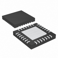
MAX9770ETI+ Maxim Integrated Products, MAX9770ETI+ Datasheet - Page 2

MAX9770ETI+
Manufacturer Part Number
MAX9770ETI+
Description
IC AMP AUDIO 1.2W MONO D 28TQFN
Manufacturer
Maxim Integrated Products
Type
Class Dr
Datasheet
1.MAX9770ETIT.pdf
(22 pages)
Specifications of MAX9770ETI+
Output Type
1-Channel (Mono) with Stereo Headphones
Max Output Power X Channels @ Load
1.2W x 1 @ 8 Ohm; 80mW x 2 @ 16 Ohm
Voltage - Supply
2.5 V ~ 5.5 V
Features
Depop, Input Multiplexer, Mute, Short-Circuit and Thermal Protection, Shutdown
Mounting Type
Surface Mount
Package / Case
28-TQFN Exposed Pad
Lead Free Status / RoHS Status
Lead free / RoHS Compliant
ABSOLUTE MAXIMUM RATINGS
GND to PGND to CPGND......................................-0.3V to +0.3V
V
V
PV
CPV
CPV
SV
C1N..........................................(PV
HPOUT_ to GND ....................................................................±3V
All Other Pins to GND.................................-0.3V to (V
Continuous Current Into/Out of:
Duration of HPOUT_ Short Circuit to V
1.2W, Low-EMI, Filterless, Mono Class D Amplifier
with Stereo DirectDrive Headphone Amplifiers
ELECTRICAL CHARACTERISTICS
(V
speaker load connected between OUT+ and OUT-, headphone load connected between HPOUT_ and GND, T
unless otherwise noted. Typical values are at T
Stresses beyond those listed under “Absolute Maximum Ratings” may cause permanent damage to the device. These are stress ratings only, and functional
operation of the device at these or any other conditions beyond those indicated in the operational sections of the specifications is not implied. Exposure to
absolute maximum rating conditions for extended periods may affect device reliability.
2
GENERAL
Supply Voltage Range
Quiescent Supply Current
Shutdown Supply Current
Shutdown to Full Operation
Input Impedance
Bias Voltage
Feedthrough
SPEAKER AMPLIFIER (GAIN1 = GAIN2 = V
Output Offset Voltage
Power-Supply Rejection Ratio
Output Power
DD
DD
DD
PV
PV
GND, PGND ...........................................................Continuous
DD
SS
_______________________________________________________________________________________
DD
SS
to PV
to GND ...........................................................................+6V
DD
SS
to GND ...........................................................................-6V
= PV
to PGND .......................................................................+6V
to CPGND....................................................................-6V
to CPGND..................................................................+6V
..............................................................................260mA
, PGND, OUT_ ......................................................600mA
DD
DD
PARAMETER
to CPV
= CPV
DD
DD
..........................................-0.3V to +0.3V
= 3.3V, GND = PGND = CPGND = 0V, SHDN = 3.3V, C1 = C2 = 1µF, C
SS
- 0.3V) to (CPGND + 0.3V)
SYMBOL
DD
I
V
PSRR
P
SHDN
V
V
, PV
t
I
R
BIAS
OUT
ON
DD
DD
OS
IN
DD
DD
A
,
= +25°C.) (Notes 1, 2)
, HPS = GND)
Inferred from PSRR test
No load
SHDN = HPS = GND
(Note 3)
From any unselected input to any output,
f = 10kHz
(Note 4)
f = 1kHz,
THD+N = 1%,
GAIN1 = 1,
GAIN2 = 0
DD
+ 0.3V)
V
T
V
V
V
A
DD
RIPPLE
RIPPLE
RIPPLE
CONDITIONS
= +25°C
= 2.5V to 5.5V,
V
V
DD
DD
= 200mV
= 200mV
= 200mV
Duration of Short Circuit Between
Duration of OUT_ Short Circuit to V
Duration of Short Circuit Between OUT+ and OUT-...............10s
Continuous Power Dissipation (T
Junction Temperature ......................................................+150°C
Operating Temperature Range ...........................-40°C to +85°C
Storage Temperature Range .............................-65°C to +150°C
Lead Temperature (soldering, 10s) .................................+300°C
MONO
INL_, INR_
Headphone mode
Speaker mode
= 3.3V
= 5V
HPOUTL and HPOUTR ..........................................Continuous
28-Pin TQFN (derate 20.8mW/°C above +70°C) .......1667mW
28-Pin TSSOP (derate 12.8mW°C above +70°C) ......1026mW
P-P
P-P
P-P
R
R
R
, f = 217Hz
, f = 1kHz
, f = 20kHz
L
L
L
= 8Ω
= 4Ω
= 8Ω
BIAS
MIN
2.5
1.1
14
50
7
= 0.047µF, SYNC = GND, R
A
= +70°C)
DD
1200
, PV
TYP
1.25
±15
550
900
5.5
5.2
0.1
50
10
20
70
70
70
68
50
DD
, GND, PGND ..10s
A
= T
MAX
±70
5.5
7.5
1.4
10
10
MIN
to T
UNITS
mW
L
mA
mV
ms
kΩ
dB
dB
µA
V
V
MAX
= ∞,
,


