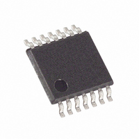
MAX4410EUD+ Maxim Integrated Products, MAX4410EUD+ Datasheet - Page 16

MAX4410EUD+
Manufacturer Part Number
MAX4410EUD+
Description
IC AMP AUDIO .08W STER 14TSSOP
Manufacturer
Maxim Integrated Products
Series
DirectDrive™r
Type
Class ABr
Datasheet
1.MAX4410EBET.pdf
(20 pages)
Specifications of MAX4410EUD+
Output Type
Headphones, 2-Channel (Stereo)
Max Output Power X Channels @ Load
80mW x 2 @ 16 Ohm
Voltage - Supply
1.8 V ~ 3.6 V
Features
Depop, Short-Circuit and Thermal Protection, Shutdown
Mounting Type
Surface Mount
Package / Case
14-TSSOP
Product
Audio Line Drivers / Receivers
Output Power
80 mW
Thd Plus Noise
0.003 %
Supply Current
7 mA
Maximum Power Dissipation
727 mW
Maximum Operating Temperature
+ 85 C
Mounting Style
SMD/SMT
Audio Load Resistance
16 Ohms
Input Offset Voltage
0.5 mV
Minimum Operating Temperature
- 40 C
Amplifier Class
AB
No. Of Channels
2
Supply Voltage Range
1.8V To 3.6V
Load Impedance
16ohm
Operating Temperature Range
-40°C To +85°C
Amplifier Case Style
TSSOP
Rohs Compliant
Yes
Lead Free Status / RoHS Status
Lead free / RoHS Compliant
80mW, DirectDrive Stereo Headphone Driver
with Shutdown
Figure 5. MAX4410 and MAX5408 Volume Control Circuit
16
The output capacitor value and ESR directly affect the
ripple at PV
put ripple. Likewise, decreasing the ESR of C2
reduces both ripple and output resistance. Lower
capacitance values can be used in systems with low
maximum output power levels. See the Output Power
vs. Charge-Pump Capacitance and Load Resistance
graph in the Typical Operating Characteristics.
The power-supply bypass capacitor (C3) lowers the out-
put impedance of the power supply, and reduces the
impact of the MAX4410’s charge-pump switching tran-
sients. Bypass PV
place it physically close to the PV
(refer to the MAX4410 EV kit for a suggested layout).
The addition of a digital potentiometer provides simple
volume control. Figure 5 shows the MAX4410 with the
MAX5408 dual log taper digital potentiometer used as
an input attenuator. Connect the high terminal of the
MAX5408 to the audio input, the low terminal to ground
and the wiper to C
tion passes the audio signal unattenuated. Setting the
wiper to the lowest position fully attenuates the input.
______________________________________________________________________________________
SS
. Increasing the value of C2 reduces out-
DD
IN
LEFT AUDIO
RIGHT AUDIO
Power-Supply Bypass Capacitor
with C3, the same value as C1, and
. Setting the wiper to the top posi-
INPUT
INPUT
Adding Volume Control
12
6
11
5
H0
H1
L0
L1
Output Capacitor (C2)
MAX5408
DD
and PGND pins
W1A 10
W0A 7
C
C
IN
IN
R
R
IN
IN
Proper layout and grounding are essential for optimum
performance. Connect PGND and SGND together at a
single point on the PC board. Connect all components
associated with the charge pump (C2 and C3) to the
PGND plane. Connect PV
device. Connect PV
device. Bypassing of both supplies is accomplished
by charge-pump capacitors C2 and C3 (see Typical
Application Circuit). Place capacitors C2 and C3 as
close to the device as possible. Route PGND and all
traces that carry switching transients away from SGND
and the traces and components in the audio signal
path. Refer to the layout example in the MAX4410 EV
kit datasheet.
When using the MAX4410 in a UCSP package, make
sure the traces to OUTR (bump C2) are wide enough
to handle the maximum expected current flow. Multiple
traces may be necessary.
For general UCSP information and PC layout consider-
ations, refer to the Maxim Application Note: Wafer-
Level Ultra Chip-Scale Package.
10
13
INL
INR
MAX4410
R
R
F
F
OUTR
OUTL
11
8
SS
DD
and SV
Layout and Grounding
UCSP Considerations
and SV
SS
DD
together at the
together at the


