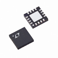
LTC6401CUD-20#PBF Linear Technology, LTC6401CUD-20#PBF Datasheet - Page 4

LTC6401CUD-20#PBF
Manufacturer Part Number
LTC6401CUD-20#PBF
Description
IC ADC DRIVER DIFF 16-QFN
Manufacturer
Linear Technology
Type
ADC Driverr
Datasheet
1.LTC6401CUD-20PBF.pdf
(16 pages)
Specifications of LTC6401CUD-20#PBF
Applications
Data Acquisition
Mounting Type
Surface Mount
Package / Case
16-WQFN Exposed Pad
No. Of Amplifiers
1
Input Offset Voltage
2mV
Gain Db Max
20dB
Bandwidth
1.3GHz
Slew Rate
4500V/µs
Supply Voltage Range
2.85V To 3.5V
Supply Current
50mA
Amplifier Case Style
QFN
Rohs Compliant
Yes
Lead Free Status / RoHS Status
Lead free / RoHS Compliant
Available stocks
Company
Part Number
Manufacturer
Quantity
Price
AC ELECTRICAL CHARACTERISTICS
LTC6401-20
fl oating, V
SYMBOL
–3dBBW
0.1dBBW
0.5dBBW
1/f
SR
t
t
t
t
–3dBBW
10MHz Input Signal
HD
IMD
OIP
P
NF
e
e
70MHz Input Signal
HD
IMD
OIP
P
NF
e
e
140MHz Input Signal
HD
4
S1%
OVDR
ON
OFF
IN,10M
ON,10M
IN,70M
ON,70M
1dB,10M
1dB,70M
10M
70M
2,10M
2,70M
2,140M
3,10M
3,70M
3,10M
3,70M
/HD
/HD
CM
/HD
OCM
3,10M
3,70M
3,140M
= 1.25V, ⎯ E ⎯ N ⎯ A ⎯ B ⎯ L ⎯ E = 0V, No R
PARAMETER
–3dB Bandwidth
Bandwidth for 0.1dB Flatness
Bandwidth for 0.5dB Flatness
1/f Noise Corner
Slew Rate
1% Settling Time
Output Overdrive Recovery Time
Turn-On Time
Turn-Off Time
Common Mode Small Signal –3dB
BW
Second/Third Order Harmonic
Distortion
Third-Order Intermodulation
(f1 = 9.5MHz f2 = 10.5MHz)
Third-Order Output Intercept Point
(f1 = 9.5MHz f2 = 10.5MHz)
1dB Compression Point
Noise Figure
Input Referred Voltage Noise Density
Output Referred Voltage Noise Density Includes Resistors (Short Inputs)
Second/Third Order Harmonic
Distortion
Third-Order Intermodulation
(f1 = 69.5MHz f2 = 70.5MHz)
Third-Order Output Intercept Point
(f1 = 69.5MHz f2 = 70.5MHz)
1dB Compression Point
Noise Figure
Input Referred Voltage Noise Density
Output Referred Voltage Noise Density Includes Resistors (Short Inputs)
Second/Third Order Harmonic
Distortion
L
unless otherwise noted.
CONDITIONS
200mV
200mV
200mV
Differential (Note 6)
2V
1.9V
+OUT, –OUT Within 10% of Final Values
I
0.1V
Output (Note 6)
2V
2V
2V
2V
2V
2V
2V
R
R
Includes Resistors (Short Inputs)
2V
2V
2V
2V
2V
2V
2V
R
R
Includes Resistors (Short Inputs)
2V
2V
2V
CC
L
L
L
L
P-P,OUT
P-P,OUT
P-P,OUT
P-P,OUTFILT
P-P,OUT
P-P,OUT
P-P,OUTFILT
P-P,OUT
P-P,OUT
P-P,OUT
P-P,OUTFILT
P-P,OUT
P-P,OUT
P-P,OUTFILT
P-P,OUT
P-P,OUT
P-P,OUT
P-P,OUTFILT
= 375Ω (Notes 5, 7)
= 375Ω (Note 5)
= 375Ω (Notes 5, 7)
= 375Ω (Note 5)
Falls to 10% of Nominal
P-P,OUT
P-P
P-P,OUT
P-P,OUT
P-P,OUT
at V
, R
, No R
, R
, No R
, R
, No R
(Note 6)
Composite, R
Composite, No R
Composite, No R
Composite, R
Composite, No R
Composite, No R
(Note 6)
OCM
L
L
L
, No R
, No R
, No R
Composite, No R
Composite, No R
= 400Ω
= 400Ω
= 400Ω
Specifi cations are at T
(Note 6)
(Note 6)
(Note 6)
L
L
L
, Measured Single-Ended at
L
L
L
L
L
= 400Ω
= 400Ω
L
L
L
L
(Note 7)
(Note 7)
L
L
A
= 25°C. V
MIN
+
= 3V, V
–110/–103
–113/–102
–122/–92
–
–91/–80
–95/–88
–95/–88
–80/–57
–81/–60
–80/–65
= 0V, +IN and –IN
4500
–108
–105
1.25
12.5
17.3
50.5
17.3
TYP
130
250
146
–96
–88
–93
–92
6.2
2.1
6.1
2.1
78
15
58
21
21
2
7
MAX
nV/√ ⎯ H ⎯ z
nV/√ ⎯ H ⎯ z
nV/√ ⎯ H ⎯ z
nV/√ ⎯ H ⎯ z
UNITS
640120f
dBm
dBm
dBm
dBm
MHz
MHz
V/μs
MHz
GHz
kHz
dBc
dBc
dBc
dBc
dBc
dBc
dBc
dBc
dBc
dBc
dBc
dBc
dBc
dBc
dBc
dB
dB
ns
ns
ns
ns


