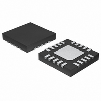
MAX3272AETP+ Maxim Integrated Products, MAX3272AETP+ Datasheet - Page 7

MAX3272AETP+
Manufacturer Part Number
MAX3272AETP+
Description
IC AMP LIMITING 20-TQFN
Manufacturer
Maxim Integrated Products
Type
Limiting Amplifierr
Datasheet
1.MAX3272AETP.pdf
(14 pages)
Specifications of MAX3272AETP+
Applications
Optical Networks
Mounting Type
Surface Mount
Package / Case
20-TQFN Exposed Pad
Input Voltage Range (max)
1200 mV
Operating Supply Voltage
3.3 V
Supply Current
33 mA
Operating Temperature Range
- 40 C to + 85 C
Mounting Style
SMD/SMT
Power Dissipation
1100 mW
Amplifier Type
Low Power
Supply Voltage Range
3V To 3.6V
Amplifier Case Style
TQFN
No. Of Pins
20
Termination Type
SMD
Supply Voltage Min
3V
Rohs Compliant
Yes
Filter Terminals
SMD
Lead Free Status / RoHS Status
Lead free / RoHS Compliant
Two control voltages V
the LOS assert and deassert levels. To prevent LOS
chatter in the region of the programmed threshold,
approximately 3.3dB of hysteresis is built into the LOS
assert/deassert function. Once asserted, LOS is not
deasserted until the input amplitude rises to the
required level (V
To facilitate interfacing with +5V modules, the LOS and
LOS pins on the MAX3272 do not have internal ESD
protection. If ESD protection is desired, a low-capaci-
tance Schottky diode or diode array structure, such as
the MAX3202E, is recommended (see the Typical
Operating Circuits).
The LOS and LOS pins on the MAX3272A include ESD
protection and, as a result, cannot be interfaced with
+5V modules.
The high-bandwidth gain stage provides approximately
42dB of gain.
Figure 3. Input Circuit
0.25pF
0.25pF
IN+
IN-
STRUCTURES
ESD
DEASSERT
_______________________________________________________________________________________
ASSERT
540Ω
110Ω
).
V
GND
CC
, and V
540Ω
DEASSERT
Gain Stage
, define
+3.3V, 2.5Gbps Low-Power
Due to the high gain of the amplifier, the MAX3272/
MAX3272A are susceptible to DC offsets in the signal
path. In communications systems using NRZ data with
a 50% duty cycle, pulse-width distortion present in the
signal or generated by the transimpedance amplifier
appears as input offset and is removed by the offset-
cancellation loop. An external capacitor is required
between CAZ1 and CAZ2 to decouple the offset-can-
cellation loop and determine the lower 3dB frequency
of the signal path.
Figure 4a. LOS Output Circuit for MAX3272
Figure 4b. LOS Output Circuit for MAX3272A
Limiting Amplifiers
Interface Schematics
GND
GND
V
V
CC
CC
Offset-Correction Loop
8kΩ
8kΩ
ESD
STRUCTURE
ESD
STRUCTURE
LOS
LOS
7


