SY88793VKG Micrel Inc, SY88793VKG Datasheet - Page 3
SY88793VKG
Manufacturer Part Number
SY88793VKG
Description
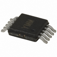
IC POST AMP PECL LP LIMIT 10MSOP
Manufacturer
Micrel Inc
Type
Limiting Postamplifierr
Datasheet
1.SY88793VKG.pdf
(8 pages)
Specifications of SY88793VKG
Applications
Optical Networks
Mounting Type
Surface Mount
Package / Case
10-MSOP, Micro10™, 10-uMAX, 10-uSOP
Lead Free Status / RoHS Status
Lead free / RoHS Compliant
Other names
576-2547
SY88793VKG
SY88793VKG
Available stocks
Company
Part Number
Manufacturer
Quantity
Price
Company:

Part Number:
SY88793VKG
Manufacturer:
Micrel Inc
Quantity:
135


Micrel, Inc.
Absolute Maximum Ratings
Supply Voltage (V
Input Voltage (D
Output Current (I
EN Voltage ............................................................. 0 to V
V
SD
Lead Temperature (soldering, 20 sec.) ................... +260 C
Storage Temperature (T
Note 1.
Note 2.
Note 3.
V
Symbol
I
SD
V
V
I
I
V
V
V
V
V
V
V
Note 1.
Note 2.
Note 3.
M9999-072505
hbwhelp@micrel.com or (408) 955-1690
CC
IH
IL
CC
IH
IL
IHCMR
REF
REF
OH
OL
OH
OL
OFFSET
DC ELECTRICAL CHARACTERISTICS
Continuous ............................................................. 50mA
Surge .................................................................... 100mA
LVL
LVL
= 3.0V to 3.6V or 4.5V to 5.5V; R
Current ......................................... –800 A to +500 A
Voltage ................................................. V
Permanent device damage may occur if ABSOLUTE MAXIMUM RATINGS are exceeded. This is a stress rating only and functional operation is
not implied at conditions other than those detailed in the operational sections of this data sheet. Exposure to ABSOLUTE MAXIMUM RATlNG
conditions for extended periods may affect device reliability.
The data sheet limits are not guaranteed if the device is operated beyond the operating ratings.
Commercial devices are guaranteed from 0 C to +85 C ambient temperature.
Specification for packaged product only.
The V
The current provided into or from V
IHCMR
Parameter
Power Supply Current
SD
EN Input HIGH Voltage
EN Input LOW Voltage
EN Input HIGH Current
EN Input LOW Current
SD Output HIGH Level
SD Output LOW Level
PECL Output HIGH Voltage
PECL Output LOW Voltage
Differential Output Offset
Common Mode Range
Reference Voltage
IN
LVL
OUT
CC
, /D
range is referenced to the most positive side of the differential input signal.
Voltage
) ....................................... 0V to +7.0V
)
IN
) .........................................0 to V
S
) ....................... –55 C to +125 C
LOAD
REF
(Note 1)
= 50 to V
must be limited to 800 A source and 500 A sink.
REF
CC
Condition
no output load
V
V
V
V
V
I
50 to V
50 to V
Note 2
Note 3
OL
IN
IN
IN
CC
CC
(Note 1)
–2V; T
= +2mA
to V
= 2.7V
= V
= 0.5V
> 3.3V
< 3.3V
CC
CC
CC
CC
CC
CC
A
= –40 C to +85 C; typical values at V
–2V output load
–2V output load
3
Operating Ratings
Supply Voltage (V
Ambient Temperature (T
Junction Temperature (T
Package Thermal Resistance
MSOP
............................................................ +4.5V to +5.5V
JA
JB
) Still-Air .................................................. 113 C/W
) Still-Air .................................................... 74 C/W
CC
) .............................. +3.0V to +3.6V or
V
V
GND +1.7
V
CC
CC
CC
V
–0.3
Min
A
J
2.0
2.4
2.0
–1.085 V
–1.830 V
REF
(Note 2)
–1.38
), Note 3 .......... –40 C to +120 C
), Note 3 ............ –40 C to +85 C
CC
= 3.3V, T
V
CC
CC
CC
Typ
25
–0.955 V
–1.705 V
–1.32
A
= 25 C.
V
CC
CC
CC
Max
V
100
V
0.8
0.5
42
20
–0.880
–1.555
100
–1.26
CC
CC
SY88793V
Units
mA
mA
mV
V
V
V
V
V
V
V
V
V
V
A
A
Related parts for SY88793VKG
Image
Part Number
Description
Manufacturer
Datasheet
Request
R

Part Number:
Description:
Manufacturer:
Micrel Inc
Datasheet:
Part Number:
Description:
Manufacturer:
Micrel Inc
Datasheet:
Part Number:
Description:
Manufacturer:
Micrel Inc
Datasheet:
Part Number:
Description:
Manufacturer:
Micrel Inc
Datasheet:
Part Number:
Description:
Manufacturer:
Micrel Inc
Datasheet:
Part Number:
Description:
Manufacturer:
Micrel Inc
Datasheet:
Part Number:
Description:
Manufacturer:
Micrel Inc
Datasheet:
Part Number:
Description:
Manufacturer:
Micrel Inc
Datasheet:
Part Number:
Description:
Manufacturer:
Micrel Inc
Datasheet:
Part Number:
Description:
Manufacturer:
Micrel Inc
Datasheet:
Part Number:
Description:
Manufacturer:
Micrel Inc
Datasheet:
Part Number:
Description:
Manufacturer:
Micrel Inc
Datasheet:
Part Number:
Description:
Manufacturer:
Micrel Inc
Datasheet:
Part Number:
Description:
Manufacturer:
Micrel Inc
Datasheet: