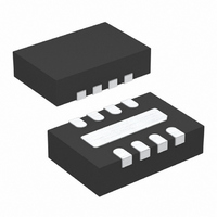
LT6552IDD#PBF Linear Technology, LT6552IDD#PBF Datasheet - Page 5

LT6552IDD#PBF
Manufacturer Part Number
LT6552IDD#PBF
Description
IC AMP VIDEO DIFF 3.3V 8-DFN
Manufacturer
Linear Technology
Datasheet
1.LT6552CS8PBF.pdf
(16 pages)
Specifications of LT6552IDD#PBF
Applications
Differential
Number Of Circuits
1
-3db Bandwidth
75MHz
Slew Rate
600 V/µs
Current - Supply
14mA
Current - Output / Channel
70mA
Voltage - Supply, Single/dual (±)
3 V ~ 12.6 V, ±1.5 V ~ 6.3 V
Mounting Type
Surface Mount
Package / Case
8-WFDFN Exposed Pad
Lead Free Status / RoHS Status
Lead free / RoHS Compliant
Available stocks
Company
Part Number
Manufacturer
Quantity
Price
5V ELECTRICAL CHARACTERISTICS
ing temperature range, otherwise specifications are at T
V
SYMBOL
V
I
I
e
i
R
CMRR
PSRR
G
SR
FPBW
BW
t
t
I
I
V
V
temperature range, otherwise specifications are at T
V
SYMBOL
t
t
B
OS
n
r
S
SC
S
ON
OFF
n
OS
, t
L
H
DIFF
V
IN
E
DIFF
5V ELECTRICAL CHARACTERISTICS
OS
f
/ T
= 0V, V
= 0V, V
SHDN
SHDN
= V
= V
PARAMETER
Input Offset Voltage
Input V
Input Bias Current
Input Offset Current
Input Noise Voltage Density
Input Noise Current Density
Input Resistance
Common Mode Rejection Ratio
Input Range
Power Supply Rejection
Gain Error
Output Voltage Swing
Slew Rate
Full-Power Bandwidth
Small-Signal –3dB Bandwidth
Rise Time, Fall Time
Settling Time to 3%
Settling Time to 1%
Differential Gain
Differential Phase
Short-Circuit Current
Supply Current Shutdown
Supply Current
Shutdown Pin Input Low Voltage
Shutdown Pin Input High Voltage
PARAMETER
Turn-On Time
Turn-Off Time
Shutdown Output Leakage Current
+
+
, unless otherwise noted. R
, unless otherwise noted. R
OS
Drift
CONDITIONS
Both Inputs (Note 7)
Any Input
Either Input Pair
f = 10kHz
f = 10kHz
Common Mode, V
V
V
V
(V
R
R
R
V
V
V
A
A
A
R
A
A
V
0 C T
–40 C T
V
L
L
CM
S
O
L
L
L
CM
O
O
V
V
V
L
V
V
OUT
SHDN
DIFF
= R
= R
= 2, V
= 2, R
= 2, R
= 2V to 6V, V
= 1k
= 150
= 75 , 0 C T
= 2, R
= 50, V
= 150
= –3V to 3V, R
= –5V to 5V Measure from –2V to 2V, R
= 6V
A
= –5V to 3V
= 0V, V
= 25 C. V
= 0V, V
F
F
= 0.6V), V
= –4.5V
CONDITIONS
V
V
V
A
A
P-P
+ R
+ R
SHDN
SHDN
SHDN
L
L
L
= 25 C. V
O
A
OUT
= 150 , Output Black Level = 0V
= 150 , Output Black Level = 0V
= 150
(Note 9)
70 C
G
G
DIFF
= –3V to 3V, 20% to 80%
DIFF
= 1k. (Note 6)
= 1k. (Note 6)
from 0.5V to 4.7V
from 4.7V to 0.5V
= 0.5V, 0V V
85 C
= 6V, Positive Step
= –1.5V to +1.5V,
S
R
= 1V
L
L
The
CM
= 5V, 0V. Figure 1 shows the DC test circuit, V
REF
A
CM
= 1k
= 150
The
S
= –5V to 3V
(Pin 1) = 0V, A
= 0V
70 C (Only)
= 5V. Figure 2 shows the DC test circuit, V
denotes the specifications which apply over the full operating
denotes the specifications which apply over the full operat-
OUT
V
+
V
= 10
L
= 150
MIN
MIN
400
2.75
4.7
58
–5
48
50
45
35
4.8
3.6
4.875
0.25
TYP
0.15
TYP
300
600
125
650
250
450
REF
0.7
0.2
10
50
25
55
75
54
30
75
25
35
70
14
4.3
3.4
1
1
1
REF
= V
= V
CM
LT6552
CM
1400
MAX
MAX
–4.5
16.5
18.5
175
25
30
50
5
3
3
3
= 1V,
= 0V,
nV/ Hz
pA/ Hz
UNITS
UNITS
5
V/ C
V/ s
MHz
MHz
6552f
Deg
mV
mV
mA
mA
mA
mA
mA
k
dB
dB
ns
ns
ns
ns
ns
%
%
%
A
A
V
V
V
V
A
V
V
A


