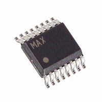
MAX9503GEEE+T Maxim Integrated Products, MAX9503GEEE+T Datasheet - Page 2

MAX9503GEEE+T
Manufacturer Part Number
MAX9503GEEE+T
Description
IC VIDEO AMP W/FILTER 16-QSOP
Manufacturer
Maxim Integrated Products
Series
DirectDrive™r
Datasheet
1.MAX9503GEEET.pdf
(13 pages)
Specifications of MAX9503GEEE+T
Applications
Filter
Number Of Circuits
1
Current - Supply
12mA
Current - Output / Channel
50mA
Voltage - Supply, Single/dual (±)
2.7 V ~ 3.6 V
Mounting Type
Surface Mount
Package / Case
16-SSOP (0.150", 3.90mm Width)
Lead Free Status / RoHS Status
Lead free / RoHS Compliant
Other names
MAX9503GEEE+TTR
ABSOLUTE MAXIMUM RATINGS
V
VIDIN to SGND .........................................................-0.3V to +4V
BIAS to SGND ............................................-0.3V to (V
SHDN to SGND ........................................................-0.3V to +4V
VIDOUT to SGND........................(The greater of V
CPV
C1P, C1N, CPV
CPGND, SGND, GND............................................-0.1V to +0.1V
CPV
DirectDrive Video Amplifier with
Reconstruction Filter
Stresses beyond those listed under “Absolute Maximum Ratings” may cause permanent damage to the device. These are stress ratings only, and functional
operation of the device at these or any other conditions beyond those indicated in the operational sections of the specifications is not implied. Exposure to
absolute maximum rating conditions for extended periods may affect device reliability.
ELECTRICAL CHARACTERISTICS
(V
R
V
2
Supply Voltage Range
Quiescent Supply Current
Shutdown Supply Current
Bias Voltage
VIDEO AMPLIFIER
Input Voltage Range
Input Current
Input Resistance
DC Voltage Gain (Note 2)
Output Black Level (Note 3)
Output Voltage Swing
Output Short-Circuit Current
Output Resistance
Shutdown Output Impedance
DD
DD
L
DD
= 150Ω to SGND, unless otherwise noted. V
DD
SS
_______________________________________________________________________________________
to SGND............................................................-0.3V to +4V
= CPV
= CPV
to V
to CPGND ....................................................-0.3V to +4V
PARAMETER
SS ..................................................................
DD
DD
= SHDN = 3.0V, T
SS
=
.............................Capacitor Connection Only
SHDN = 3.0V, SGND = GND = CPGND = 0V, C1 = C2 = C3 = C4 = 1µF, R
A
= +25°C, unless otherwise noted.) (Note 1)
R
SYMBOL
V
OUTSHDN
CPV
I
V
R
RANGE
V
SHDN
I
R
BIAS
I
A
I
OUT
DD
DD
SC
IN
IN
V
DD
,
-0.1V to +0.1V
SS
Guaranteed by DC voltage gain, V
VIDIN
Guaranteed by DC voltage gain and
quiescent current
V
V
SHDN = SGND
Guaranteed by DC
voltage gain, V
Guaranteed by DC
voltage gain, V
V
V
V
Guaranteed by DC voltage gain, V
Sinking or sourcing
MAX9503G
MAX9503M
SHDN = SGND
(V
DD
DD
DD
DD
DD
and -2V) to
DD
DD
= 3.6V (I
= 3.6V (I
= 2.7V
= 2.7V to 3.6V
= 2.7V
= 286mV (MAX9503G), V
+ 0.3V)
+ 0.3V)
DD
SHDN
DD
DD
CONDITIONS
= I
= 2.7V
= 3V
= I
VDD
VIDOUT Short Circuit to V
Continuous Current
Continuous Power Dissipation (T
Operating Temperature Range ...........................-40°C to +85°C
Junction Temperature ......................................................+150°C
Storage Temperature Range .............................-65°C to +150°C
Lead Temperature (soldering, 10s) .................................+300°C
VDD
and the Greater of (V
VIDIN, BIAS, SHDN ......................................................±20mA
16-Pin QSOP (derate 8.3mW/°C above +70°C)...........667mW
16-Pin TQFN (derate 15.6mW/°C above +70°C) .......1349mW
+ I
MAX9503G
MAX9503M
CPVDD
+ I
MAX9503G
MAX9503M
MAX9503G
MAX9503M
MAX9503G
MAX9503M
MAX9503G
MAX9503M
CPVDD
VIDIN
, R
DD
DD
),
L
= 2.7V
= ∞)
= 143mV (MAX9503M). Typical values are at
= 3V
SS
DD
and -2V) ...........................Continuous
-0.050
2.162
2.594
-0.10
-0.10
-0.05
-0.15
MIN
11.5
-2.5
-0.1
, SGND
2.7
5.5
BIAS
A
= 100kΩ, T
= +70°C)
TYP
0.01
0.01
0.02
4.2
8.2
12
12
50
1
1
6
0
0
A
+0.525
+1.05
+1.28
+0.64
+0.15
MAX
+2.5
+0.1
12.5
3.6
6.5
= T
15
1
MIN
to T
UNITS
V
MΩ
mA
mA
dB
kΩ
µA
µA
P-P
Ω
V
V
V
V
MAX
.


