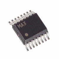
MAX9541AEE+ Maxim Integrated Products, MAX9541AEE+ Datasheet - Page 13

MAX9541AEE+
Manufacturer Part Number
MAX9541AEE+
Description
IC AMP VIDEO MUX 2:1 16-QSOP
Manufacturer
Maxim Integrated Products
Datasheet
1.MAX9541AEE.pdf
(16 pages)
Specifications of MAX9541AEE+
Applications
2:1 Multiplexer-Amplifier
Number Of Circuits
4
Current - Supply
21mA
Current - Output / Channel
140mA
Voltage - Supply, Single/dual (±)
2.7 V ~ 3.6 V
Mounting Type
Surface Mount
Package / Case
16-SSOP (0.150", 3.90mm Width)
Lead Free Status / RoHS Status
Lead free / RoHS Compliant
The video output amplifiers can both source and sink
load current, allowing output loads to be DC- or
AC-coupled. The amplifier output stage needs approxi-
mately 300mV of headroom from either supply rail. The
devices have an internal level-shift circuit that positions
the sync tip at approximately 300mV at the output.
If the supply voltage is greater than 3.135V (5% below
a 3.3V supply), each amplifier can drive two DC-cou-
pled video loads to ground. If the supply is less than
3.135V, each amplifier can drive only one DC-coupled
or AC-coupled video load.
The outputs can be AC-coupled since the output stage
can source and sink current as shown in Figure 3.
Coupling capacitors should be 220µF or greater to
keep the highpass filter, formed by the 150Ω equivalent
resistance of the video transmission line, to a corner
frequency of 4.8Hz or below. The frame rate of PAL
systems is 25Hz, the frame rate of NTSC systems is
30Hz, and the frame rate of VGA is usually 60Hz or
higher. The corner frequency should be well below the
frame rate.
Table 4. Quiescent and Average Power Consumption
Quiescent power consumption
Average power consumption
TOP VIEW
MEASUREMENT
IN0A
IN1A
IN2A
IN3A
IN0B
IN1B
IN2B
IN3B
Applications Information
______________________________________________________________________________________
1
2
6
3
4
5
7
8
+
AC-Coupling the Outputs
MAX9541
MAX9542
QSOP
Standard-Definition and VGA Signals
Pin Configuration
Quadruple, 2:1, Mux Amplifiers for
POWER CONSUMPTION (mW)
16
15
14
13
12
11
10
9
V
A/B
OUT0
OUT1
OUT2
OUT3
SHDN
GND
DD
Outputs
175
69
The quiescent power consumption and average power
consumption of the MAX9541/MAX9542 are very low
because of 3.3V operation and low-power circuit
design. Quiescent power consumption is defined when
the MAX9541/MAX9542 are operating without loads
and without any video signals.
Average power consumption represents the normal power
consumption when the devices drive real video signals
into real video loads. It is measured when the MAX9541/
MAX9542 drive 150Ω loads to ground with a 50% flat
field, which serves as proxy for a real video signal.
Table 4 shows the quiescent and average power con-
sumption of the MAX9541/MAX9542.
The MAX9541/MAX9542 operate from a single-supply
voltage down to 2.7V, allowing for low-power operation.
Bypass V
external components as close as possible to the
device.
PROCESS: BiCMOS
No load.
150Ω to ground on each output. 50% flat field signal on
each input.
Power-Supply Bypassing and Ground
DD
to GND with a 0.1µF capacitor. Place all
CONDITIONS
Chip Information
Power Consumption
13


