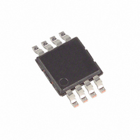
MAX9650AUA+ Maxim Integrated Products, MAX9650AUA+ Datasheet - Page 5

MAX9650AUA+
Manufacturer Part Number
MAX9650AUA+
Description
IC OP AMP VCOM DRIVE 8-UMAX-EP
Manufacturer
Maxim Integrated Products
Datasheet
1.MAX9650AUA.pdf
(13 pages)
Specifications of MAX9650AUA+
Applications
TFT-LCD Panels: VCOM Driver
Output Type
Rail-to-Rail
Number Of Circuits
1
-3db Bandwidth
35MHz
Slew Rate
40 V/µs
Current - Supply
3.7mA
Current - Output / Channel
1.3A
Voltage - Supply, Single/dual (±)
9 V ~ 20 V, ±4.5 V ~ 10 V
Mounting Type
Surface Mount
Package / Case
8-TSSOP, 8-MSOP (0.118", 3.00mm Width), Exposed Pad
Lead Free Status / RoHS Status
Lead free / RoHS Compliant
The MAX9650/MAX9651 operational rail-to-rail
input/output amplifiers hold the VCOM voltage stable
while providing the ability to source and sink a high cur-
rent quickly (1.3A) into a capacitive load such as the
backplane of a TFT-LCD panel.
The MAX9650/MAX9651 are capable of high output
currents and feature thermal-shutdown protection with
temperature hysteresis. When the die temperature
reaches +170°C, the device shuts down. When the die
cools down by 15°C, the device turns on again. In a
TFT-LCD application, the duty cycle is very low. Even
with high values of voltage and current, the power dissi-
pation is low and the chip does not shut down.
SOT23
—
—
—
—
—
1
2
3
4
5
MAX9650
µMAX-EP,
TDFN-EP
1, 5, 8
—
—
—
—
6
4
3
2
7
PIN
with Temperature Hysteresis
_______________________________________________________________________________________
(µMAX-EP,
TDFN-EP)
MAX9651
Detailed Description
—
—
1
4
3
2
8
5
6
7
Thermal Shutdown
High-Current VCOM Drive Op Amps
NAME
OUTA
OUTB
INA+
INB+
GND
INA-
INB-
N.C.
V
EP
DD
VCOM Output A
Ground
Positive Input A
Negative Input A
Positive-Supply Input. Bypass V
possible to the device.
Positive Input B
Negative Input B
VCOM Output B
No Connection. Not internally connected.
Exposed Pad (μMAX and TDFN Only). EP is internally connected to GND. Connect EP
to GND.
Figure 1. Settling Time Test Circuit
V
REF
SUPPLY
19V
**(R
*10μF and 0.1μF CAPACITORS AS CLOSE AS POSSIBLE TO THE PIN.
*C2 = 0.1μF
DD
S
= R
to GND with a 0.1µF capacitor as close as
GEN
FUNCTION
IN_+
IN_-
) x C
SUPPLY
19V
LCD
MAX9650
x 6 < 2μs, WHERE R
GND
V
DD
for TFT LCDs
OUT_
*C1 = 10μF
GEN
V
Pin Description
OUT_
= GENERATOR SOURCE IMPEDANCE.
R
2.2Ω
S
=
LCD VCOM LOAD
**0V TO 2.2V
AT 50kHz
C
0.1μF
LCD
=
5


