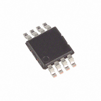
MAX4158EUA+ Maxim Integrated Products, MAX4158EUA+ Datasheet - Page 2

MAX4158EUA+
Manufacturer Part Number
MAX4158EUA+
Description
IC VIDEO MUX/AMP 8-UMAX
Manufacturer
Maxim Integrated Products
Datasheet
1.MAX4158EUA.pdf
(16 pages)
Specifications of MAX4158EUA+
Applications
2:1 Multiplexer-Amplifier
Number Of Circuits
1
-3db Bandwidth
350MHz
Slew Rate
700 V/µs
Current - Supply
10.9mA
Current - Output / Channel
100mA
Voltage - Supply, Single/dual (±)
±4.5 V ~ 5.5 V
Mounting Type
Surface Mount
Package / Case
8-TSSOP, 8-MSOP (0.118", 3.00mm Width)
Lead Free Status / RoHS Status
Lead free / RoHS Compliant
ABSOLUTE MAXIMUM RATINGS
350MHz/250MHz, 2-Channel
Video Multiplexer-Amplifiers
Positive Supply Voltage (V+ to GND) ...................................+6V
Negative Supply Voltage (V- to GND).....................................-6V
Amplifier Input Voltage (IN0 or IN1) .....(V- - 0.3V) to (V+ + 0.3V)
FB Current ........................................................................±20mA
Digital Input Voltage (A0,
Output Short Circuit to GND (Note 1).........................Continuous
Output Short-Circuit Current to V+, V- (Note 1)........................5s
Stresses beyond those listed under “Absolute Maximum Ratings” may cause permanent damage to the device. These are stress ratings only, and functional
operation of the device at these or any other conditions beyond those indicated in the operational sections of the specifications is not implied. Exposure to
absolute maximum rating conditions for extended periods may affect device reliability.
DC ELECTRICAL CHARACTERISTICS
(V+ = +5V, V- = -5V, V
2
Note 1: Continuous power dissipation maximum rating must also be observed.
Operating Supply-Voltage Range
Input Voltage Range
Input Offset Voltage (Either Channel)
Input Offset Voltage Temperature
Coefficient (Either Channel)
Input Bias Current (Channel On)
FB Pin Bias Current
Input Resistance
FB Pin Input Resistance
Output Resistance
Disabled Output Resistance
Open-Loop Transimpedance
DC Common-Mode Rejection Ratio
DC Power-Supply Rejection Ratio
Output Voltage Swing
Output Current
Output Short-Circuit Current
Positive Supply Current
Negative Supply Current
_______________________________________________________________________________________
PARAMETER
IN
= 0V, V
EN, or LE) ............-0.3V to (V+ + 0.3V)
OUT
= 0V, R
SYMBOL
R
TCV
R
CMRR
V+, V-
R
PSRR
V
OUT(d)
I
V
IN(FB)
V
R
OUT
I
I
I
OUT
OUT
Z
SC
I+
FB
OS
IN
I-
IN
IN
T
L
OS
= , T
Inferred from the PSRR test
Inferred from the CMRR test
T
T
T
T
V
f = 0Hz
MAX4159/MAX4259 only, EN = 5V,
V
V
V
Open loop, V+ = +4.5V to +5.5V,
V- = -4.5V to -5.5V
R
R
V
Sinking or sourcing to ground
MAX4158/MAX4258
EN = GND, MAX4159/MAX4259
EN = V+, MAX4159/MAX4259
MAX4158/MAX4258
EN = GND, MAX4159/MAX4259
EN = V+, MAX4159/MAX4259
A
A
A
A
A
IN
OUT
OUT
IN
OUT
L
L
= T
= +25°C
= T
= +25°C
= T
= open circuit
= 50Ω
= -2.5V to 2.5V
= -2.5V to 2.5V
= -3.0V to 3.0V (Note 2)
= -2.5V to 2.5V, R
= -2.5V to 2.5V
MIN
MIN
MIN
to T
to T
to T
CONDITIONS
MAX
MAX
MAX
, unless otherwise noted. Typical values are at T
Continuous Power Dissipation (T
Operating Temperature Range ...........................-40°C to +85°C
Storage Temperature Range .............................-65°C to +160°C
Lead Temperature (soldering, 10s) .................................+300°C
8-Pin SO (derate 5.88mW/°C above +70°C).................471mW
8-Pin µMAX (derate 4.10mW/°C above +70°C) ............330mW
14-Pin SO (derate 8.33mW/°C above +70°C)...............667mW
16-Pin QSOP (derate 8.33mW/°C above +70°C)..........667mW
L
= 100Ω
Channel on
Channel off
±4.5
±2.5
±3.0
±2.5
MIN
100
1.0
50
60
70
1
1
A
= +70°C)
±3.0
±4.0
±3.5
TYP
10.9
10.9
550
100
120
3.0
6.3
9.9
9.9
5.0
±1
±2
±2
20
50
40
10
60
78
2
MAX
±5.5
13.0
13.0
12.0
12.0
±10
±18
±12
±20
8.0
7.0
A
±6
= +25°C.)
UNITS
µV/°C
MΩ
mΩ
MΩ
MΩ
mA
mA
mA
mA
mV
µA
µA
kΩ
dB
dB
Ω
V
V
V


