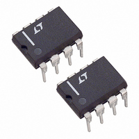
LT1192CN8#PBF Linear Technology, LT1192CN8#PBF Datasheet - Page 3

LT1192CN8#PBF
Manufacturer Part Number
LT1192CN8#PBF
Description
IC OP-AMP VIDEO HI-SPD SNGL 8DIP
Manufacturer
Linear Technology
Datasheet
1.LT1192CN8.pdf
(12 pages)
Specifications of LT1192CN8#PBF
Applications
General Purpose
Number Of Circuits
1
Slew Rate
450 V/µs
Current - Supply
32mA
Current - Output / Channel
50mA
Voltage - Supply, Single/dual (±)
4.75 V ~ 16 V, ±2.38 V ~ 8 V
Mounting Type
Through Hole
Package / Case
8-DIP (0.300", 7.62mm)
Lead Free Status / RoHS Status
Lead free / RoHS Compliant
Available stocks
Company
Part Number
Manufacturer
Quantity
Price
ELECTRICAL CHARACTERISTICS
V
SYMBOL
V
I
I
CMRR
A
V
SR
GBW
I
I
The
V
SYMBOL
V
I
I
CMRR
PSRR
A
V
I
I
SYMBOL
Diff A
Diff Ph
I
I
t
t
OS
B
S
SHDN
OS
B
S
SHDN
S
SHDN
ON
OFF
S
OS
VOL
OUT
S
OS
VOL
OUT
V
+
OS
= 5V, Pin 5 open circuit unless otherwise noted.
= 5V, V
V
/ T
denotes the specifications which apply over the full operating temperature range of – 55 C T
S
–
PARAMETER
Input Offset Voltage
Input Offset Current
Input Bias Current
Input Voltage Range
Common Mode Rejection Ratio
Large-Signal Voltage Gain
Output Voltage Swing
Slew Rate
Gain Bandwidth Product
Supply Current
Shutdown Supply Current
Shutdown Pin Current
PARAMETER
Input Offset Voltage
Input V
Input Offset Current
Input Bias Current
Common Mode Rejection Ratio
Power Supply Rejection Ratio
Large-Signal Voltage Gain
Output Voltage Swing
Supply Current
Shutdown Supply Current
Shutdown Pin Current
PARAMETER
Differential Gain
Differential Phase
Supply Current
Shutdown Supply Current
Shutdown Pin Current
Turn On Time
Turn Off Time
= 0V, V
OS
CM
Drift
= 2.5V, T
A
= 25 C, C
L
10pF, Pin 5 open circuit unless otherwise noted.
CONDITIONS
N8 Package
V
V
R
R
R
Pin 5 at V
Pin 5 at V
CONDITIONS
All Packages
(Note 3)
V
R
R
A
Pin 5 at V
Pin 5 at V
CONDITIONS
R
R
Pin 5 at V
Pin 5 at V
Pin 5 from V
Pin 5 from Ground to V
CM
S
L
L
L
CM
V
L
L
L
L
= 2.375V to 5V
= 1k, V
= 100 , V
= 1k
= –5, V
= 100 to Ground, V
= 100 to Ground
= 150 , A
= 150 , A
= – 2.5V to 3.5V
= 2V to 3.5V
V
O
–
–
S
–
–
–
–
(Note 8)
O
= 3V
= 5V, T
O
= 1V to 3V
–
V
V
= 3V
to Ground, R
= 10 (Note 7)
= 10 (Note 7)
A
= 25 C, C
–
O
, R
= 1V to 3V
L
L
= 1k
= 1k
V
V
OUT
OUT
L
High
Low
10pF, Pin 5 open circuit unless otherwise noted.
A
MIN
MIN
MIN
3.6
60
30
65
70
55
3.7
2
5
125 C.
LT1192M/C
LT1192M/C
LT1192M
0.25
TYP
0.23
0.15
250
350
TYP
TYP
100
400
0.4
0.2
3.8
1.2
0.4
0.2
1.5
1.3
80
50
29
20
85
90
90
14
32
20
32
20
0.5
0.5
3.9
2
MAX
MAX
MAX
1.2
3.5
0.4
3.5
2.5
36
50
38
38
50
1.5
4
2
2.5
2
2
LT1192
Deg
UNITS
UNITS
UNITS
V/mV
V/mV
V/mV
V/ s
MHz
3
V/ C
mA
mA
mV
mA
mA
mV
mA
mA
P-P
dB
dB
dB
ns
ns
%
A
A
A
V
V
A
A
A
V
A


