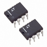
LT1190CN8#PBF Linear Technology, LT1190CN8#PBF Datasheet - Page 8

LT1190CN8#PBF
Manufacturer Part Number
LT1190CN8#PBF
Description
IC OP-AMP VIDEO HI-SPD SNGL 8DIP
Manufacturer
Linear Technology
Datasheet
1.LT1190CN8.pdf
(12 pages)
Specifications of LT1190CN8#PBF
Applications
General Purpose
Number Of Circuits
1
Slew Rate
450 V/µs
Current - Supply
32mA
Current - Output / Channel
50mA
Voltage - Supply, Single/dual (±)
4.75 V ~ 16 V, ±2.38 V ~ 8 V
Mounting Type
Through Hole
Package / Case
8-DIP (0.300", 7.62mm)
Lead Free Status / RoHS Status
Lead free / RoHS Compliant
Available stocks
Company
Part Number
Manufacturer
Quantity
Price
Power Supply Bypassing
The LT1190 is quite tolerant of power supply bypassing.
In some applications a 0.1 F ceramic disc capacitor
placed 1/2 inch from the amplifier is all that is required. A
scope photo of the amplifier output with no supply
bypassing is used to demonstrate this bypassing toler-
ance, R
LT1190
APPLICATIO S I FOR ATIO
Supply bypassing can also affect the response in the
frequency domain. It is possible to see a slight 1dB rise in
the frequency response at 130MHz depending on the gain
configuration, supply bypass, inductance in the supply
leads and printed circuit board layout. This can be further
minimized by not using a socket.
8
L
= 1k .
–10
–20
20
10
Closed-Loop Voltage Gain vs Frequency
0
100k
V
T
R
A
S
L
No Supply Bypass Capacitors
= 5V
= 25 C
= 1k
A
V
= –1, IN DEMO BOARD, R
U
1M
A
A
V
FREQUENCY (Hz)
V
= 2
= 1
U
10M
100M
L
W
= 1k
LT1190 • TA05
LT1190 • TA04
1G
U
In most applications, and those requiring good settling
time, it is important to use multiple bypass capacitors. A
0.1 F ceramic disc in parallel with a 4.7 F tantalum is
recommended. Two oscilloscope photos with different
bypass conditions are used to illustrate the settling time
characteristics of the amplifier. Note that although the
output waveform looks acceptable at 1V/DIV, when ampli-
fied to 1mV/DIV the settling time to 2mV is 4.244 s for the
0.1 F bypass; the time drops to 163ns with multiple
bypass capacitors.
1V/DIV
1V/DIV
V
V
OUT
OUT
SUPPLY BYPASS CAPACITORS = 0.1 F + 4.7 F TANTALUM
SUPPLY BYPASS CAPACITORS = 0.1 F
Settling Time Poor Bypass
Settling Time Good Bypass
SETTLING TIME TO 2mV, A
SETTLING TIME TO 2mV, A
V
V
= –1
= –1
LT1190 • TA06
LT1190 • TA07
0V
0V
V
1mV/DIV
V
1mV/DIV
OUT
OUT


