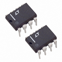
LT1193CN8 Linear Technology, LT1193CN8 Datasheet - Page 7

LT1193CN8
Manufacturer Part Number
LT1193CN8
Description
IC AMP VIDEO DIF ADJ GAIN 8-DIP
Manufacturer
Linear Technology
Datasheet
1.LT1193CN8PBF.pdf
(12 pages)
Specifications of LT1193CN8
Applications
Differential
Number Of Circuits
1
-3db Bandwidth
80MHz
Slew Rate
500 V/µs
Current - Supply
35mA
Current - Output / Channel
50mA
Voltage - Supply, Single/dual (±)
4.75 V ~ 16 V, ±2.38 V ~ 8 V
Mounting Type
Through Hole
Package / Case
8-DIP (0.300", 7.62mm)
Lead Free Status / RoHS Status
Contains lead / RoHS non-compliant
Available stocks
Company
Part Number
Manufacturer
Quantity
Price
Company:
Part Number:
LT1193CN8
Manufacturer:
LT
Quantity:
5 510
Part Number:
LT1193CN8#PBF
Manufacturer:
LINEAR/凌特
Quantity:
20 000
APPLICATIO S I FOR ATIO
TYPICAL PERFOR A CE CHARACTERISTICS
The LT1193 is a video difference amplifier which has two
uncommitted high input impedance (+) and (–) inputs.
The amplifier has one set of inputs that can be used for
reference and feedback. Additionally, this set of inputs
give gain adjust and DC control to the differential amplifier.
The voltage gain of the LT1193 is set like a conventional
operational amplifier. Feedback is applied to Pin 8 and it is
optimized for gains of 2 or greater. The amplifier can be
operated single-ended by connecting either the (+) or (–)
inputs to +/REF, Pin 1. The voltage gain is set by the
resistors: (R
The primary usefulness of the LT1193 is in converting
high speed differential signals to a single-ended output.
The amplifier has common mode rejection beyond 50MHz
–1
–3
–5
5
3
1
10
Output Voltage Swing
vs Load Resistance
Large-Signal Transient Response
V
T
A
S
A
T
V
= 5V
= –55 C
A
= 2, R
= –55 C, 25 C
L
FB
LOAD RESISTANCE ( )
= 150 , R
T
A
+ R
= 125 C
T
T
A
A
G
100
= 25 C
= 125 C
U
FB
)/R
= 300 , R
G
.
U
G
W
LT1193 • TPC19
= 300
LT1193 • TPC22
U
1000
W
900
800
700
600
500
400
300
–50
Slew Rate vs Temperature
Small-Signal Transient Response
V
T
R
V
U
A
S
L
O
A
= 25 C
= 5V
= 1k
= 2V
V
–25
= –10, SMALL-SIGNAL RISE TIME = 43ns
– SLEW RATE
0
TEMPERATURE ( C)
+SLEW RATE
25
and a full-power bandwidth of 40MHz at 4V
single-ended case, the differential voltage gain is set by the
external resistors: (R
differential signal for which the output will respond is
approximately 1.3V.
Power Supply Bypassing
The LT1193 is quite tolerant of power supply bypassing.
In some applications a 0.1 F ceramic disc capacitor
placed 1/2 inch from the amplifier is all that is required. A
scope photo of the amplifier output with no supply by-
passing is used to demonstrate this bypassing tolerance,
R
50
L
= 1k.
75
LT1193 • TPC20
LT1193 • TPC23
100
125
FB
–2
–4
4
2
0
+ R
40
Small-Signal Transient Response
Output Voltage Step
vs Settling Time, A
V
T
R
S
A
L
= 25 C
= 5V
= 1k
OVERSHOOT = 25%, RISE TIME = 4.7ns
G
50
)/R
10mV
A
V
= 2, R
G
SETTLING TIME (ns)
. The maximum input
10mV
60
FB
= 300 , R
70
V
= 2
G
LT1193
P-P
80
= 300 ,
. Like the
LT1193 • TPC21
90
LT1193 • TPC24
1193fb
7
100


