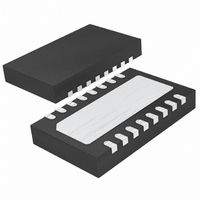
LT6557CDHC#TRPBF Linear Technology, LT6557CDHC#TRPBF Datasheet - Page 3

LT6557CDHC#TRPBF
Manufacturer Part Number
LT6557CDHC#TRPBF
Description
IC AMP VIDEO TRIPLE 16-DFN
Manufacturer
Linear Technology
Datasheet
1.LT6557CGNPBF.pdf
(12 pages)
Specifications of LT6557CDHC#TRPBF
Applications
General Purpose
Number Of Circuits
3
-3db Bandwidth
500MHz
Slew Rate
2200 V/µs
Current - Supply
22.5mA
Current - Output / Channel
70mA
Voltage - Supply, Single/dual (±)
3 V ~ 7.5 V, ±2.5 V ~ 3.3 V
Mounting Type
Surface Mount
Package / Case
16-WFDFN Exposed Pad
Lead Free Status / RoHS Status
Lead free / RoHS Compliant
Available stocks
Company
Part Number
Manufacturer
Quantity
Price
Note 1: Stresses beyond those listed under Absolute Maximum Ratings
may cause permanent damage to the device. Exposure to any Absolute
Maximum Rating condition for extended periods may affect device
reliability and lifetime.
Note 2: A heat sink may be required to keep the junction temperature
below the Absolute Maximum Rating.
Note 3: The LT6557C is guaranteed functional over the temperature range
of –40°C and 85°C.
Note 4: The LT6557C is guaranteed to meet specifi ed performance from
0°C to 70°C. The LT6557C is designed, characterized and expected to
ELECTRICAL CHARACTERISTICS
temperature range, otherwise specifi cations are at T
otherwise noted.
SYMBOL
A
A
V
PSRR
V
V
I
I
I
SR
–3dB BW
0.1dB BW
FPBW
XTalk
t
t
ΔG
ΔΦ
HD2
HD3
S
EN
SC
S
r
V
V
, t
IN(DC)
OL
OH
ERR
MATCH
f
PARAMETER
Gain Error
Gain Match Between Channels
Input Voltage Bias
Power Supply Rejection Ratio
Output Voltage Swing Low
Output Voltage Swing High
Supply Current per Amplifi er
Total Supply Current (Disabled)
Enable Pin Current
Short-Circuit Current
Slew Rate
–3dB Bandwidth
Gain Flatness ±0.1dB Bandwidth
Full Power Bandwidth
All Hostile Crosstalk
Settling Time
Rise Time, Fall Time
Differential Gain
Differential Phase
2nd Harmonic Distortion
3rd Harmonic Distortion
A
= 25°C. V
CONDITIONS
V
V
R
V
V
(Pin 15)
V
V
V
V
V
V
V
f = 10MHz, V
f = 100MHz, V
To 1%, V
To 0.1%
10% to 90%, V
NTSC Signal
NTSC Signal
f = 10MHz, V
f = 10MHz, V
IN
IN
S
EN
EN
EN
OUT
OUT
OUT
OUT
OUT
BCV
= 4V to 6V, V
The
= 0.75V to 1.75V
= 0.75V to 1.75V
= 0.4V, R
= Open, R
= 0.4V
= 348Ω
= 1.25V to 3.75V (Note 5)
= 2V
= 0.2V
= 2V
= 2V
●
S
OUT
P-P
P-P
P-P
= 5V, R
denotes the specifi cations which apply over the full operating
P-P
OUT
OUT
OUT
= 1.5V to 3.5V
L
(Note 6)
L
OUT
= ∞, Includes I
OUT
= ∞
meet specifi ed performance from –40°C to 85°C but is not tested or
QA sampled at these temperatures.The LT6557I is guaranteed to meet
specifi ed performance from –40°C to 85°C.
Note 5: Slew rate is 100% production tested on the R channel and
measured on the rising edge of the output signal. The slew rate of the
falling edge and of the G and B channels is guaranteed through design and
characterization.
Note 6: Large-signal bandwidth is calculated from slew rate:
IN
= 2V
= 2V
= 2V
= 2V
= 1.25V
L
= 1.5V to 3.5V
FPBW = SR/(π • V
= 150Ω to V
P-P
P-P
P-P
P-P
S
of V
S
/2, V
+
P-P
)
EN
= 0.4V, R
●
●
●
●
●
●
●
●
●
●
–250
–300
1400
MIN
±70
±40
220
1.0
0.8
4.1
4.0
42
38
BCV
= open, unless
–125
–150
±100
2200
±0.5
±0.5
±0.4
±0.4
1.25
1.10
22.5
25.0
0.02
0.05
TYP
±90
400
500
120
350
–80
–55
875
–68
–75
0.8
0.9
4.2
4.1
50
47
10
10
4
7
LT6557
±2.75
±3.25
1000
MAX
±2.5
±3.0
450
1.5
1.7
0.9
1.0
25
29
UNITS
6557fa
3
V/µs
MHz
MHz
MHz
MHz
Deg
dBc
dBc
mA
mA
mA
mA
µA
µA
µA
µA
dB
dB
dB
dB
ns
ns
ps
%
%
%
%
%
V
V
V
V
V
V


