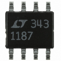
LT1187CS8#TR Linear Technology, LT1187CS8#TR Datasheet - Page 9

LT1187CS8#TR
Manufacturer Part Number
LT1187CS8#TR
Description
IC AMP VID DIFF CURR FDBK 8SOIC
Manufacturer
Linear Technology
Datasheet
1.LT1187CS8PBF.pdf
(16 pages)
Specifications of LT1187CS8#TR
Applications
Differential
Number Of Circuits
1
-3db Bandwidth
50MHz
Slew Rate
165 V/µs
Current - Supply
13mA
Current - Output / Channel
20mA
Voltage - Supply, Single/dual (±)
4.75 V ~ 16 V, ±2.38 V ~ 8 V
Mounting Type
Surface Mount
Package / Case
8-SOIC (0.154", 3.90mm Width)
Power Supply Requirement
Single/Dual
Dual Supply Voltage (typ)
±5V
Mounting
Surface Mount
Pin Count
8
Lead Free Status / RoHS Status
Contains lead / RoHS non-compliant
Lead Free Status / RoHS Status
Contains lead / RoHS non-compliant
Available stocks
Company
Part Number
Manufacturer
Quantity
Price
APPLICATIONS INFORMATION
Operating with Low Closed-Loop Gains
The LT1187 has been optimized for closed-loop gains
of 2 or greater. For a closed-loop gain of 2 the response
peaks about 2dB. Peaking can be eliminated by placing a
capacitor across the feedback resistor, (feedback zero).
This peaking shows up as time domain overshoot of
about 25%.
A
V
= 2, OVERSHOOT = 25%, R
Closed-Loop Voltage Gain vs Frequency
–1
9
8
7
6
5
4
3
2
1
0
100k
Small-Signal Transient Response
V
T
A
R
R
S
A
V
FB
G
= 25°C
= 2
= 900Ω
= ±5V
= 900Ω
C
1M
FB
FREQUENCY (Hz)
= 5pF
FB
= R
C
C
FB
G
FB
= 1k
10M
= 0pF
= 10pF
LT1187 • AI03
100M
LT1187 • AI04
Extending the Input Range
Figure 1 shows a simplifi ed schematic of the LT1187. In
normal operation REF, Pin 1, is grounded or taken to a DC
offset control voltage and differential signals are applied
between Pins 2 and 3. The input responds linearly until
all of the 345µA current fl ows through the 1.1k resistor
and Q1 (or Q2) turns off. Therefore the maximum input
swing is 380mV
pair, Q3 and Q4, is running at slightly larger current so
that when the fi rst input stage limits, the second stage
remains biased to maintain the feedback.
Occasionally it is necessary to handle signals larger than
760mV
tricked to handle up to 1.5V
to ground Pin 3 and apply the differential input signal
between Pins 1 and 2. The input signal is now applied
across two 1.1k resistors in series. Since the input signal
is applied to both input pairs, the fi rst pair will run out of
bias current before the second pair, causing the amplifi er
to go open loop. The results of this technique are shown
in the following scope photo.
P-P
A
V
= 2, WITH 8pF FEEDBACK CAPACITOR
at the input. The LT1187 input stage can be
Small-Signal Transient Response
P
or 760mV
P-P
P-P
. To do this, it is necessary
. The second differential
LT1187
LT1187 • AI05
1187fa
9


