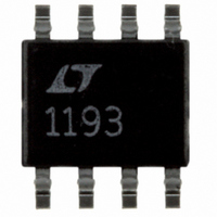
LT1193CS8#TR Linear Technology, LT1193CS8#TR Datasheet - Page 3

LT1193CS8#TR
Manufacturer Part Number
LT1193CS8#TR
Description
IC AMP VIDEO DIFF ADJUST 8SOIC
Manufacturer
Linear Technology
Datasheet
1.LT1193CN8PBF.pdf
(12 pages)
Specifications of LT1193CS8#TR
Applications
Differential
Number Of Circuits
1
-3db Bandwidth
80MHz
Slew Rate
500 V/µs
Current - Supply
35mA
Current - Output / Channel
50mA
Voltage - Supply, Single/dual (±)
4.75 V ~ 16 V, ±2.38 V ~ 8 V
Mounting Type
Surface Mount
Package / Case
8-SOIC (0.154", 3.90mm Width)
Power Supply Requirement
Single/Dual
Dual Supply Voltage (typ)
±5V
Mounting
Surface Mount
Pin Count
8
Lead Free Status / RoHS Status
Contains lead / RoHS non-compliant
Lead Free Status / RoHS Status
Contains lead / RoHS non-compliant
Available stocks
Company
Part Number
Manufacturer
Quantity
Price
ELECTRICAL CHARACTERISTICS
to ground, R
SYMBOL
I
I
t
t
V
T
SYMBOL
V
I
I
CMRR
V
SR
BW
I
I
The
V
unless otherwise noted.
SYMBOL
V
I
I
CMRR
PSRR
V
G
I
I
S
SHDN
ON
OFF
OS
B
S
SHDN
OS
B
S
SHDN
A
OS
OUT
OS
OUT
S
REF
V
E
+
OS
= 25 C, C
= 5V, V
/ T
= 0V, R
denotes the specificatons which apply over the full operating temperature range of – 55 C T
PARAMETER
Supply Current
Shutdown Supply Current
Shutdown Pin Current
Turn On Time
Turn Off Time
PARAMETER
Input Offset Voltage
Input Offset Current
Input Bias Current
Input Voltage Range
Common Mode Rejection Ratio
Output Voltage Swing
Slew Rate
Small-Signal Bandwidth
Supply Current
Shutdown Supply Current
Shutdown Pin Current
PARAMETER
Input Offset Voltage
Input V
Input Offset Current
Input Bias Current
Input Voltage Range
Common Mode Rejection Ratio
Power Supply Rejection Ratio
Output Voltage Swing
Gain Error
Supply Current
Shutdown Supply Current
Shutdown Pin Current
S
L
L
FB1
–
= R
= 0V, V
10pF, Pin 5 open circuit, unless otherwise noted.
= 900 from Pins 6 to 8, R
OS
FB1
Drift
+ R
REF
FB2
= 2.5V, R
= 1k (Note 3), T
FB1
= 900 from Pins 6 to 8, R
FB2
A
= 25 C, C
= 100 from Pin 8 to ground, R
CONDITIONS
Pin 5 at V
Pin 5 at V
Pin 5 from V
Pin 5 from Ground to V
CONDITIONS
V
V
R
V
V
Pin 5 at V
Pin 5 at V
CONDITIONS
Both Inputs (Note 4) All Packages
Either Input
Either Input
V
R
V
Pin 5 at V
Pin 5 at V
CM
S
S
O
L
CM
O
L
= 2.375V to 5V
= 1k
= 8V, R
= 3V, R
= 100 to Ground
= 1V to 3V
= – 2.5V to 3.5V
= 2V to 3.5V
L
10pF, Pin 5 open circuit, unless otherwise noted.
–
–
–
–
V
–
–
(Note 10)
L
S
L
–
= 100
= 1k
= 5V, V
to Ground, R
FB2
= 100 from Pin 8 to V
–
REF
, R
L
L
= 0V, R
= 1k
= 1k
V
V
L
OUT
OUT
= R
FB1
High
Low
FB2
= 900 from Pins 6 to 8, R
= 1k (Note 3), C
REF
, R
L
= R
A
–2.5
MIN
MIN
MIN
3.6
3.6
53
53
55
6
2
L
FB1
125 C. V
10pF, Pin 5 open circuit,
LT1193M/C/I
LT1193M/C/I
+ R
LT1193M
0.25
TYP
300
200
FB2
TYP
250
TYP
1.3
0.2
3.8
1.3
0.8
6.5
0.2
1.3
35
20
70
32
20
20
70
70
35
20
0.5
3
8
2
4
1
FB2
S
= 1k (Note 3),
= 5V,
= 100 from Pin 8
MAX
MAX
MAX
3.5
0.4
43
50
15
40
50
3.5
1.2
2.2
16
43
3.5
2
3
2
5.5
5
LT1193
UNITS
UNITS
UNITS
1193fb
3
V/ C
V/ s
MHz
mA
mA
mV
mA
mA
mV
mA
mA
dB
dB
dB
ns
ns
%
A
A
A
V
V
V
A
A
A
V
V
A


