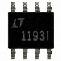
LT1193IS8#TR Linear Technology, LT1193IS8#TR Datasheet - Page 4

LT1193IS8#TR
Manufacturer Part Number
LT1193IS8#TR
Description
IC AMP VIDEO DIFF ADJ 8-SOIC
Manufacturer
Linear Technology
Datasheet
1.LT1193CN8PBF.pdf
(12 pages)
Specifications of LT1193IS8#TR
Applications
Differential
Number Of Circuits
1
-3db Bandwidth
80MHz
Slew Rate
500 V/µs
Current - Supply
35mA
Current - Output / Channel
50mA
Voltage - Supply, Single/dual (±)
4.75 V ~ 16 V, ±2.38 V ~ 8 V
Mounting Type
Surface Mount
Package / Case
8-SOIC (0.154", 3.90mm Width)
Power Supply Requirement
Single/Dual
Dual Supply Voltage (typ)
±5V
Operating Temperature Classification
Industrial
Mounting
Surface Mount
Pin Count
8
Lead Free Status / RoHS Status
Contains lead / RoHS non-compliant
Lead Free Status / RoHS Status
Contains lead / RoHS non-compliant
Available stocks
Company
Part Number
Manufacturer
Quantity
Price
ELECTRICAL CHARACTERISTICS
The
V
unless otherwise noted.
SYMBOL
V
I
I
CMRR
PSRR
V
G
I
I
LT1193
The
R
unless otherwise noted.
SYMBOL
V
I
I
CMRR
PSRR
V
G
I
I
Note 1: Absolute Maximum Ratings are those values beyond which the
life of a device may be impaired.
Note 2: A heat sink is required to keep the junction temperature below
absolute maximum when the output is shorted.
Note 3: When R
when R
output.
Note 4: V
input pair, and is input referred.
Note 5: V
Pin 3) for which the output can respond.
Note 6: Slew rate is measured between 2V on the output, with a 1V
input step, A
4
OS
B
S
SHDN
OS
B
S
SHDN
OS
OUT
REF
V
E
OS
OUT
FB1
V
E
OS
OS
/ T
= 0V, R
/ T
= 900 from Pins 6 to 8, R
denotes the specificatons which apply over the full operating temperature range of – 40 C T
denotes the specificatons which apply over the full operating temperature range of 0 C T
L
= 100 is specified, then an additional 100 is added to the
OS
IN LIM
PARAMETER
Input Offset Voltage
Input V
Input Offset Current
Input Bias Current
Input Voltage Range
Common Mode Rejection Ratio
Power Supply Rejection Ratio
Output Voltage Swing
Gain Error
Supply Current
Shutdown Supply Current
Shutdown Pin Current
V
measured at the output (Pin 6) is the contribution from both
FB1
PARAMETER
Input Offset Voltage
Input V
Input Offset Current
Input Bias Current
Input Voltage Range
Common Mode Rejection Ratio
Power Supply Rejection Ratio
Output Voltage Swing
Gain Error
Supply Current
Shutdown Supply Current
Shutdown Pin Current
= 3.
is the maximum voltage between –V
L
= 900 from Pins 6 to 8, R
= 1k is specified, the load resistor is R
OS
OS
Drift
Drift
FB2
= 100 from Pin 8 to ground, R
FB2
IN
= 100 from Pin 8 to ground, R
and +V
FB1
CONDITIONS
SO-8 Package
V
V
R
V
V
Pin 5 at V
Pin 5 at V
CONDITIONS
N8 Package
SO-8 Package
V
V
R
R
V
Pin 5 at V
Pin 5 at V
CM
S
L
S
O
CM
S
O
L
L
= 2.375V to 5V
= 1k
= 8V, R
= 3V, R
= 2.375V to 5V
= 1k
= 100
+ R
= 3V, R
= – 2.5V to 3.5V
= – 2.5V to 3.5V
IN
FB2
(Pin 2 and
, but
–
–
–
–
(Note 10)
(Note 10)
L
L
L
= 100
= 1k
= 1k
L
= R
Note 7: Full-power bandwidth is calculated from the slew rate
measurement:
Note 8: Settling time measurement techniques are shown in “Take the
Guesswork Out of Settling Time Measurements,” EDN, September 19,
1985.
Note 9: NTSC (3.58MHz).
Note 10: See Applications section for shutdown at elevated temperatures.
Do not operate the shutdown above T
Note 11: AC parameters are 100% tested on the ceramic and plastic DIP
packaged parts (J and N suffix) and are sample tested on every lot of the
SO packaged parts (S suffix).
FB1
FPBW = SR/2 V
+ R
L
FB2
= R
= 1k (Note 3), C
FB2
= 1k (Note 3), C
P
.
A
L
A
–2.5
MIN
–2.5
MIN
70 C. V
3.6
3.7
6.2
53
53
55
55
6
10pF, Pin 5 open circuit,
L
J
85 C. V
> 125 C.
10pF, Pin 5 open circuit,
LT1193C
LT1193I
S
TYP
= 5V, V
TYP
0.8
6.5
0.2
1.3
0.2
6.6
0.2
1.3
20
70
70
35
20
20
70
70
35
20
S
0.5
2
4
2
4
1
= 5V,
REF
MAX
MAX
3.5
1.2
2.2
3.5
3.5
1.2
2.1
20
43
14
20
43
5.5
5
4
= 0V,
UNITS
UNITS
1193fb
V/ C
V/ C
mV
mA
mA
mV
mV
mA
mA
dB
dB
dB
dB
%
%
A
A
V
V
A
A
A
V
V
V
A


