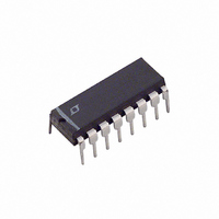
LT1204CN#PBF Linear Technology, LT1204CN#PBF Datasheet - Page 4

LT1204CN#PBF
Manufacturer Part Number
LT1204CN#PBF
Description
IC VIDEO MUX CFA 75MHZ 4IN 16DIP
Manufacturer
Linear Technology
Datasheet
1.LT1204CSWPBF.pdf
(20 pages)
Specifications of LT1204CN#PBF
Applications
4:1 Multiplexer-Amplifier
Number Of Circuits
1
-3db Bandwidth
75MHz
Slew Rate
1000 V/µs
Current - Supply
19mA
Current - Output / Channel
125mA
Voltage - Supply, Single/dual (±)
10 V ~ 30 V, ±5 V ~ 15 V
Mounting Type
Through Hole
Package / Case
16-DIP (0.300", 7.62mm)
Lead Free Status / RoHS Status
Lead free / RoHS Compliant
Available stocks
Company
Part Number
Manufacturer
Quantity
Price
AC CHARACTERISTICS
LT1204
The
temperature range.
Note 1: Analog and digital inputs (Pins 1, 3, 5, 7, 9, 10, 11 and 12) are
protected against ESD and overvoltage with internal SCRs. For inputs
< 6V the SCR will not fire, voltages above 6V will fire the SCRs and
the DC current should be limited to 50mA. To turn off the SCR the pin
voltage must be reduced to less than 2V or the current reduced to less
than 10mA.
Note 2: A heat sink may be required depending on the power supply
voltage.
Note 3: Commercial grade parts are designed to operate over the
temperature range of – 40 C to 85 C but are neither tested nor
guaranteed beyond 0 C to 70 C. Industrial grade parts specified and
tested over – 40 C to 85 C are available on special request. Consult
factory.
Note 4: T
dissipation P
Note 5: The supply current of the LT1204 has a negative temperature
coefficient. For more information see Typical Performance
Characteristics.
Note 6: Apply 0.5V DC to Pin 1 and measure the time for the
appearance of 5V at Pin 15 when Pin 9 goes from 5V to 0V. Pin 10
Voltage = 0V. Apply 0.5V DC to Pin 3 and measure the time for the
appearance of 5V at Pin 15 when Pin 9 goes from 0V to 5V. Pin 10
Voltage = 0V. Apply 0.5V DC to Pin 5 and measure the time for the
SYMBOL
t
SR
t
4
r
S
, t
f
LT1204CN: T
LT1204CS: T
denotes specifications which apply over the specified operating
J
is calculated from the ambient temperature T
PARAMETER
Small-Signal Rise and Fall Time
Slew Rate (Note 10)
Channel Select Output Transient
Settling Time
All Hostile Crosstalk (Note 11)
Disable Crosstalk (Note 11)
Shutdown Crosstalk (Note 11)
All Hostile Crosstalk (Note 11)
Disable Crosstalk (Note 11)
Shutdown Crosstalk (Note 11)
Differential Gain (Note 12)
Differential Phase (Note 12)
D
according to the following formulas:
J
J
= T
= T
A
A
+ (P
+ (P
D
D
)(90 C/W)
)(70 C/W)
T
CONDITIONS
R
R
All V
0.1%, V
SO PCB #028, R
SO PCB #028, Pin 11 Voltage = 0V, R
SO PCB #028, Pin 12 Voltage = 0V, R
PDIP PCB #029, R
PDIP PCB #029, Pin 11 Voltage = 0V, R
PDIP PCB #029, Pin 12 Voltage = 0V, R
V
V
V
V
A
L
L
S
S
S
S
= 25 C, V
= 15V, R
= 5V, R
= 15V, R
= 5V, R
= 150 , V
= 400
IN
= 0V, R
OUT
A
and power
= 10V, R
L
L
S
L
L
OUT
= 150
= 150
L
= 150
= 150
= 15V, R
= 400 , Input Referred
L
= 125mV
= 100 , R
L
= 100 , R
L
= 1k
F
S
= R
= 10
appearance of 5V at Pin 15 when Pin 9 goes from 5V to 0V. Pin 10
Voltage = 5V. Apply 0.5V DC to Pin 7 and measure the time for the
appearance of 5V at Pin 15 when Pin 9 goes from 0V to 5V. Pin 10
Voltage = 5V.
Note 7: Apply 0.5V DC to Pin 1 and measure the time for the
disappearance of 5V at Pin 15 when Pin 11 goes from 5V to 0V.
Pins 9 and 10 are at 0V.
Note 8: Apply 0.5V DC to Pin 1 and measure the time for the
appearance of 5V at Pin 15 when Pin 11 goes from 0V to 5V.
Pins 9 and 10 are at 0V. Above a 1MHz toggle rate, t
Note 9: Apply 0.5V DC at Pin 1 and measure the time for the
appearance of 5V at Pin 15 when Pin 12 goes from 0V to 5V.
Pins 9 and 10 are at 0V. Then measure the time for the disappearance
of 5V DC to 500mV at Pin 15 when Pin 12 goes from 5V to 0V.
Note 10: Slew rate is measured at 5V on a 10V output signal while
operating on 15V supplies with R
Note 11: V
4th input selected. For Disable crosstalk and Shutdown crosstalk all 4
inputs are driven simultaneously. A 6dB output attenuator is formed by
a 50 series output resistor and the 50 input impedance of the
HP4195A Network Analyzer. R
Note 12: Differential Gain and Phase are measured using a Tektronix
TSG120 YC/NTSC signal generator and a Tektronix 1780R Video
Measurement Set. The resolution of this equipment is 0.1% and 0.1 .
Five identical MUXs were cascaded giving an effective resolution of
0.02% and 0.02 .
S
= 10
G
= 1k, unless otherwise noted.
L
L
= 100 , R
= 100 , R
L
L
= 100 , R
= 100 , R
IN
= 0dBm (0.223V
S
S
= 50
= 50
S
S
= 50
= 50
RMS
F
= R
) at 10MHz on any 3 inputs with the
MIN
400
F
G
= 2k, R
= 1k.
G
1000
0.04
0.04
0.06
0.12
TYP
5.6
40
70
92
95
92
76
81
76
= 220 and R
en
MAX
reduces.
L
= 400 .
UNITS
V/ s
DEG
DEG
mV
dB
dB
dB
dB
dB
dB
ns
ns
%
%


