AD8013AR-14 Analog Devices Inc, AD8013AR-14 Datasheet - Page 11

AD8013AR-14
Manufacturer Part Number
AD8013AR-14
Description
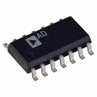
IC OPAMP SINGLE SUPPLY 14-SOIC
Manufacturer
Analog Devices Inc
Datasheet
1.AD8013ARZ-14.pdf
(12 pages)
Specifications of AD8013AR-14
Slew Rate
1000 V/µs
Mounting Type
Surface Mount
Rohs Status
RoHS non-compliant
Applications
Current Feedback
Number Of Circuits
3
-3db Bandwidth
140MHz
Current - Supply
3.5mA
Current - Output / Channel
30mA
Voltage - Supply, Single/dual (±)
4.2 V ~ 13 V, ±2.1 V ~ 6.5 V
Package / Case
14-SOIC (0.154", 3.90mm Width)
No. Of Amplifiers
3
Bandwidth
280MHz
Amplifier Case Style
SOIC
No. Of Pins
14
Settling Time
18ns
Operating Temperature Max
85°C
Lead Free Status / RoHS Status
Contains lead / RoHS non-compliant
Available stocks
Company
Part Number
Manufacturer
Quantity
Price
Company:
Part Number:
AD8013AR-14
Manufacturer:
AD
Quantity:
46
Company:
Part Number:
AD8013AR-14
Manufacturer:
ADI
Quantity:
297
Part Number:
AD8013AR-14
Manufacturer:
ADI/亚德诺
Quantity:
20 000
Company:
Part Number:
AD8013AR-14-REEL
Manufacturer:
LT
Quantity:
124
Part Number:
AD8013AR-14-REEL
Manufacturer:
ADI/亚德诺
Quantity:
20 000
REV. A
Disable Mode Operation
Pulling the voltage on any one of the Disable pins about 1.6 V
up from the negative supply will put the corresponding
amplifier into a disabled, powered down, state. In this
condition, the amplifier’s quiescent current drops to about
0.3 mA, its output becomes a high impedance, and there is
a high level of isolation from input to output. In the case of
the gain of two line driver for example, the impedance at the
output node will be about the same as for a 1.6 k resistor
(the feedback plus gain resistors) in parallel with a 12 pF
capacitor and the input to output isolation will be about
66 dB at 5 MHz.
Leaving the Disable pin disconnected (floating) will leave
the corresponding amplifier operational, in the enabled
state. The input impedance of the disable pin is about 40 k
in parallel with a few picofarads. When driven to 0 V, with
the negative supply at –5 V, about 100 A flows into the
disable pin.
When the disable pins are driven by complementary output
CMOS logic, on a single 5 V supply, the disable and enable
times are about 50 ns. When operated on dual supplies,
level shifting will be required from standard logic outputs to
the Disable pins. Figure 36 shows one possible method
which results in a negligible increase in switching time.
Figure 34. Closed-Loop Gain Matching vs. Frequency
Figure 35. Group Delay and Group Delay Matching
vs. Frequency, G = +2, R
–0.5
–1.0
–0.5
–1.0
–1.5
–2.0
1.0
0.5
1.5
1.0
0.5
10
100k
6
4
8
2
0
0
1M
G = +2
R
G = +2
R
L
L
V
= 150
= 150
S
= 5V
V
S
= +5V
10M
1M
FREQUENCY – Hz
FREQUENCY – Hz
MATCHING
DELAY
DELAY
L
= 150
V
S
= 5V
10M
100M
V
V
V
S
S
S
G = +2
R
= +5V
= +5V
= 5V
L
= 150
100M
1G
–11–
The AD8013’s input stages include protection from the large
differential input voltages that may be applied when disabled.
Internal clamps limit this voltage to about
output isolation will be maintained for voltages below this limit.
3:1 Video Multiplexer
Wiring the amplifier outputs together will form a 3:1 mux with
excellent switching behavior. Figure 37 shows a recommended
configuration which results in –0.1 dB bandwidth of 35 MHz
and OFF channel isolation of 60 dB at 10 MHz on 5 V
supplies. The time to switch between channels is about 50 ns.
Switching time is virtually unaffected by signal level.
Figure 36. Level Shifting to Drive Disable Pins on Dual
Supplies
Figure 37. A Fast Switching 3:1 Video Mux (Supply
Bypassing Not Shown)
Figure 38. Channel Switching Characteristic for the
3:1 Mux
DISABLE 2
DISABLE 3
DISABLE 1
V
V
V
IN
IN
IN
1
2
3
100
0%
90
10
V
665
665
665
I
V
V
75
75
75
500mV
5V
I
I
HIGH => AMPLIFIER ENABLED
LOW => AMPLIFIER DISABLED
8k
4k
845
13
12
10
6
9
5
845
845
+V
3
4
1
2
S
–V
11
S
10k
14
7
8
+5V
–5V
TO DISABLE PIN
84
84
84
200ns
3 V. The high input to
CABLE
75
AD8013
75
V
OUT


