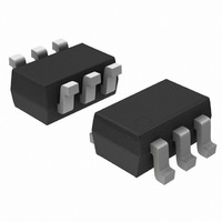
NCS2561SQT1G ON Semiconductor, NCS2561SQT1G Datasheet - Page 6

NCS2561SQT1G
Manufacturer Part Number
NCS2561SQT1G
Description
IC OP AMP HS W/FILTER SC-88
Manufacturer
ON Semiconductor
Datasheet
1.NCS2561SQT1G.pdf
(11 pages)
Specifications of NCS2561SQT1G
Applications
Filter
Number Of Circuits
1
Current - Supply
6mA
Current - Output / Channel
50mA
Voltage - Supply, Single/dual (±)
2.7 V ~ 3.3 V
Mounting Type
Surface Mount
Package / Case
6-TSSOP, SC-88, SOT-363
Lead Free Status / RoHS Status
Lead free / RoHS Compliant
Available stocks
Company
Part Number
Manufacturer
Quantity
Price
Part Number:
NCS2561SQT1G
Manufacturer:
ON/安森美
Quantity:
20 000
portable applications with low power consumption in a
space saving SC−88 package. It includes sag correction
circuitry allowing significant reduction of the AC−coupled
output capacitor.
Internal Level Shift
specifications V
(GND) and extends to V
of 2.7 V to 3.3 V. Many video processors operate with a
supply ranging from 0 V to a positive supply (typically
3.3 V), so the lowest voltage of the video signal provided by
the DAC is 0 V. Although a 0 V (GND) signal is within the
input common−mode range of the NCS2561, the output
signal will be limited, specifically at the lower rail. Op amps
use transistors with saturation voltage (Vsat) higher than
0 V. If the lowest level of the input voltage is lower than Vsat
the signal will be clipped at the output.
Shutdown Mode
enabled. The Enable pin offers a shutdown function, so the
NCS2561 can consequently be disabled when not used. This
is particularly important for digital still cameras or cell
phones with camera having a video output feature. Indeed
The NCS2561 is a single video driver optimized for
The
If the Enable pin is left open by default the circuit will be
Video
DAC
input
Cs: Optional
Rs
1 V
0 V
IN
common
) of the NCS2561 includes the lower rail
Cs
CC
Figure 10. Block Diagram Showing Filter and Sag Correction Circuits
− 1.5V on a power supply range
mode
IN
NCS2561
1.1 kW
voltage
1.4 kW
2.7V to 3.3V
12 pF
APPLICATIONS INFORMATION
V
CC
GND
range
10 pF
http://onsemi.com
650 W
+
−
325 W
(see
Enable
6
rail limit, the NCS2561 has built−in level shift circuitry. The
role of this circuitry is to avoid clipping of the sync signal at
the output by shifting up the video signal by about 60 mV.
The level shift circuitry level shifts the sync signal above the
internal op amp transistor saturation limit. This function is
particularly useful when the video signal is DC−coupled at
the output.
Built−in 2−Pole Reconstruction Filter
−3 dB cut−off frequency at 8 MHz. The filter serves as an
anti−alias filter removing the unwanted over−sampling
effects produced by the video DAC. The 27 MHz
over−sampling frequency from the video DAC is attenuated
by 22 dB typical. In order to improve the stop−band
attenuation a small capacitor (Cs) of a few tenths pico Farads
can be added in parallel with the source resistor (Rs) (See
Figure 10).
this video output is not permanently used and actually used
in very specific period of time when pictures or small movies
want to be displayed on a bigger screen. The device’s
quiescent current drops typically down to 2.7 mA when the
device is in the shutdown mode.
To ensure the output signal is not clipped due to the lower
The NCS2561 has a 2−pole reconstruction filter with a
845 W
528 W
OUT
SAG
47 mF / 67 mF
22 mF
75 W
TV
75 W


