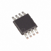
MAX4030EEUA+ Maxim Integrated Products, MAX4030EEUA+ Datasheet - Page 2

MAX4030EEUA+
Manufacturer Part Number
MAX4030EEUA+
Description
IC OP AMP DUAL 144MHZ 8-UMAX
Manufacturer
Maxim Integrated Products
Datasheet
1.MAX4030EESA.pdf
(12 pages)
Specifications of MAX4030EEUA+
Applications
General Purpose
Output Type
Rail-to-Rail
Number Of Circuits
2
-3db Bandwidth
144MHz
Slew Rate
115 V/µs
Current - Supply
12mA
Current - Output / Channel
100mA
Voltage - Supply, Single/dual (±)
4.5 V ~ 5.5 V
Mounting Type
Surface Mount
Package / Case
8-TSSOP, 8-MSOP (0.118", 3.00mm Width)
Number Of Channels
2
Voltage Gain Db
80 dB
Common Mode Rejection Ratio (min)
50 dB
Input Offset Voltage
13 mV
Operating Supply Voltage
5 V
Maximum Power Dissipation
362 mW
Maximum Operating Temperature
+ 85 C
Mounting Style
SMD/SMT
Minimum Operating Temperature
- 40 C
Lead Free Status / RoHS Status
Lead free / RoHS Compliant
ABSOLUTE MAXIMUM RATINGS
(All voltages referenced to GND, unless otherwise noted.)
V
IN_-, IN_+, OUT_,
Current into IN_-, IN_+, SHDN..........................................±20mA
Output Short-Circuit Duration to V
Continuous Power Dissipation (T
DC ELECTRICAL CHARACTERISTICS
(V
at T
Low-Cost, 144MHz, Dual/Triple Op Amps
with ±15kV ESD Protection
Stresses beyond those listed under “Absolute Maximum Ratings” may cause permanent damage to the device. These are stress ratings only, and functional
operation of the device at these or any other conditions beyond those indicated in the operational sections of the specifications is not implied. Exposure to
absolute maximum rating conditions for extended periods may affect device reliability.
2
Operating Supply Voltage Range
Quiescent Current (per Amplifier)
Shutdown Current (per Amplifier)
Input Common-Mode Voltage
Input Offset Voltage
Input Offset Voltage Matching
Input Offset Voltage Tempco
Input Bias Current
Input Offset Current
Input Resistance
Common-Mode Rejection Ratio
Power-Supply Rejection Ratio
Open-Loop Gain
Output Voltage Swing
Output Short-Circuit Current
SHDN_ Logic Threshold
SHDN_ Logic Input Current
CC
CC
8-Pin µMAX (derate 4.5mW/°C above +70°C) .............362mW
8-Pin SO (derate 5.9mW/°C above +70°C)..................471mW
A
...........................................................................-0.3V to +6V
_______________________________________________________________________________________
= 5V, V
= +25°C.) (Note 1)
PARAMETER
CM
= 0V, V
SHDN_ ..........................-0.3V to (V
OUT_
= V
A
CC
CC
= +70°C)
/2, SHDN_ = V
or GND ............Continuous
SYMBOL
TC
CMRR
V
I
PSRR
A
SHDN
V
V
V
I
I
R
OUT_
V
I
V
V
I
I
CC
I
OS
VOL
SC
CM
CC
OS
IH
VOS
IL
B
IN
IH
IL
OS
Guaranteed by PSRR
SHDN_ = GND (MAX4031E)
Guaranteed by CMRR
T
T
GND
4.5V
0.5V
0.6V
0.4V
R
R
R
Sinking or sourcing
MAX4031E
MAX4031E
SHDN_ = GND (MAX4031E)
SHDN_ = V
CC
A
A
L
L
L
CC
= +25°C
= -40°C to +85°C
, R
= 2k to V
= 150 to V
= 150 to GND
L
+ 0.3V)
V
V
V
V
V
=
CC
OUT_
OUT_
OUT_
CM
CC
to V
5.5V
CC
V
CC
(MAX4031E)
CC
4.5V, R
4.4V, R
3.5V, R
CC
CONDITIONS
/2
/2
/2, T
- 2.25V
Operating Temperature Range ...........................-40°C to +85°C
Junction Temperature .....................................................+150°C
Storage Temperature Range .............................-65°C to +150°C
Lead Temperature (soldering, 10s) .................................+300°C
14-Pin TSSOP (derate 9.1mW/°C above +70°C) .........727mW
14-Pin SO (derate 8.3mW/°C above +70°C)................667mW
L
L
L
A
V
V
V
V
V
V
= 2k to V
= 150 to V
= 150 to GND
CC
OL
CC
OL
CC
OL
= T
- GND
- GND
- GND
- V
- V
- V
MIN
OH
OH
OH
to T
CC
MAX
CC
/2
/2
, unless otherwise noted. Typical values are
MIN
4.5
2.0
50
40
50
50
0
±100
TYP
0.01
0.01
0.05
0.05
0.15
0.15
0.01
0.10
0.10
0.1
2.6
0.3
12
31
70
60
80
70
70
5
1
V
MAX
2.25
0.05
5.5
0.4
0.4
0.8
0.8
CC
22
10
13
26
10
10
1
-
UNITS
µV/°C
mA
G
mA
mV
mV
µA
µA
µA
dB
dB
dB
µA
V
V
V
V


