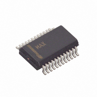
MAX9511CEG+ Maxim Integrated Products, MAX9511CEG+ Datasheet - Page 13

MAX9511CEG+
Manufacturer Part Number
MAX9511CEG+
Description
IC INTERFACE VGA 24-QSOP
Manufacturer
Maxim Integrated Products
Type
RGBHV Driverr
Datasheet
1.MAX9511CEGT.pdf
(15 pages)
Specifications of MAX9511CEG+
Applications
Driver
Number Of Circuits
3
Slew Rate
1100 V/µs
Current - Supply
38mA
Current - Output / Channel
40mA
Voltage - Supply, Single/dual (±)
4.5 V ~ 5.5 V
Mounting Type
Surface Mount
Package / Case
24-QSOP
Operating Supply Voltage
4.5 V to 5.5 V
Maximum Operating Temperature
+ 70 C
Maximum Power Dissipation
762 mW
Minimum Operating Temperature
0 C
Mounting Style
SMD/SMT
Lead Free Status / RoHS Status
Lead free / RoHS Compliant
The MAX9511 operates with a 4.5V to 5.5V power sup-
ply for video (RGBHV), while DDC and SYNC operate
from 2.3V to 3.6V and 4.5V to 5.5V supplies.
The output impedance, R
additional capacitance (C
ter that reduces the jitter of the sync output signal. With
R
of the lowpass filter is given by:
Choose C
quency of interest.
SO
TOP VIEW
(55Ω typ) sync output impedance, the -3dB point
SYNC Bandwidth-Limiting Capacitors
DDC_DATA_IN
DDC_CLK_IN
SYNC
H_SYNC_IN
V_SYNC_IN
GREEN_IN
BLUE_IN
RED_IN
AGND
SHDN
V
V
DD2
so f
RX
CC
f
-3dB
______________________________________________________________________________________
10
11
12
1
2
3
4
5
6
7
8
9
-3dB
=
MAX9511
2π
QSOP
is well above the highest fre-
SYNC
SO
R
Pin Configuration
RGBHV Driver with EMI Suppression
SO SYNC
, of the MAX9511 and an
1
) can form a lowpass fil-
C
24
23
22
21
20
19
18
17
16
15
14
13
Power Supplies
AGND
GREEN_OUT
AGND
RED_OUT
AGND
BLUE_OUT
DGND
DDC_DATA_OUT
DDC_CLK_OUT
H_SYNC_OUT
V_SYNC_OUT
V
DD1
The MAX9511’s high-frequency performance requires
proper layout and bypassing. For best performance,
place components as close to the device as possible.
Digital or AC transient signals on AGND can create
noise at the outputs. Return AGND to the lowest imped-
ance ground available. Bypass the analog supply
(V
and 0.001µF capacitor to AGND, placed as close to the
device as possible. Bypass the digital supplies (V
V
to the device as possible. Careful PC board ground lay-
out minimizes crosstalk between the outputs.
TRANSISTOR COUNT: 353
PROCESS: BIPOLAR
DD2
CC
) with a 4.7µF capacitor paralleled with a 0.22µF
) with a 0.1µF capacitor to DGND, placed as close
Power-Supply Bypassing and
Chip Information
Ground Management
DD1
13
,


