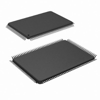
CLC5903VLA/NOPB National Semiconductor, CLC5903VLA/NOPB Datasheet - Page 22

CLC5903VLA/NOPB
Manufacturer Part Number
CLC5903VLA/NOPB
Description
IC DGTL TUNER/AGC DUAL 128-PQFP
Manufacturer
National Semiconductor
Type
Tunerr
Datasheet
1.CLC5903SMNOPB.pdf
(29 pages)
Specifications of CLC5903VLA/NOPB
Applications
Base Stations
Mounting Type
Surface Mount
Package / Case
128-MQFP, 128-PQFP
Lead Free Status / RoHS Status
Lead free / RoHS Compliant
Other names
*CLC5903VLA
*CLC5903VLA/NOPB
CLC5903VLA
*CLC5903VLA/NOPB
CLC5903VLA
Available stocks
Company
Part Number
Manufacturer
Quantity
Price
Company:
Part Number:
CLC5903VLA/NOPB
Manufacturer:
Texas Instruments
Quantity:
10 000
www.national.com
Control Register Addresses and Defaults
Condensed CLC5903 Address Map
AGC_IC_B
AGC_RB_A
AGC_RB_B
TEST_REG
Reserved
Reserved
DEBUG_EN
DEBUG_TAP
DITH_A
DITH_B
AGC_TABLE
F1_COEFF
F2_COEFF
COEF_SEL_F1A
COEF_SEL_F1B
PAGE_SEL_F1
COEF_SEL_F2A
COEF_SEL_F2B
PAGE_SEL_F2
SFS_MODE
SDC_EN
AGC_COMB_ORD
EXT_DELAY
DEC
Register Name
Register Name
a. These are the default values set by a master reset (MR). Sync in (SI) will not affect any of these values.
Width
32B
22B
64B
14b
1B
1B
1B
1B
1B
1b
5b
1b
1b
1b
1b
1b
1b
1b
1b
1b
1b
2b
5b
Addr
0
Type
R/W
R/W
R/W
R/W
R/W
R/W
R/W
R/W
R/W
R/W
R/W
R/W
R/W
R/W
R/W
R/W
R/W
R/W
R/W
R
R
-
-
Addr
Hex
0x00
Default
0
0
0
0
0
0
1
1
0
0
0
0
0
0
0
0
0
0
0
0
0
-
-
Dec7
a
Bit7
28(MSBs)
27(LSBs)
128-159
160-181
182-245
Addr
246
246
246
247
247
247
248
248
249
249
24
25
26
29
30
31
31
31
31
Dec6
Bit6
Bit
7:0
7:0
7:0
7:0
5:0
7:0
7:0
5:1
7:0
7:0
7:0
1:0
6:2
0
6
7
0
1
2
0
1
2
0
1
AGC fixed gain for channel B. Format is an 8-bit, unsigned magnitude number. The channel
B DVGA gain will be set to the inverted three MSBs.
AGC integrator readback value for channel A. Format is an 8-bit, unsigned magnitude num-
ber. The user can read the magnitude MSBs of the channel A integrator from this register.
AGC integrator readback value for channel B. Format is an 8-bit, unsigned magnitude num-
ber. The user can read the magnitude MSBs of the channel B integrator from this register.
Test input source. Instead of processing values from the A|BIN pins, the value from this
location is used instead. Format is 14-bit 2s complement number spread across 2 regis-
ters.
For future use.
For future use.
0=Normal. 1=Enables access to the internal probe points.
Selects internal node tap for debug.
0 selects F1 output for BI, 20 bits
1 selects F1 output for BQ, 20 bits
2 selects F1 output for AQ, 20 bits
3 selects F1 output for AI, 20 bits
4 selects F1 input for BI, 20 bits
5 selects F1 input for BQ, 20 bits
6 selects F1 input for AI, 20 bits
7 selects F1 input for AQ, 20 bits
8 selects NCO A, cosine output. 17 bits, 3 LSBs are 0.
9 selects NCO A, sine output, 17 bits, 3 LSBs are 0.
10 selects NCO B, cosine output, 17 bits, 3 LSBs are 0.
11 selects NCO B, sine output, 17 bits, 3 LSBs are 0.
12 selects NCO AI, rounded output, 15 bits, 5 LSBs are 0.
13 selects NCO AQ, rounded output, 15 bits, 5 LSBs are 0.
14 selects NCO BI, rounded output, 15 bits, 5 LSBs are 0.
15 selects NCO BQ, rounded output, 15 bits, 5 LSBs are 0.
16-31 selects AGC CIC filter output. 9 MSBs from ch A, next 9 bits from ch B, 2 LSBs are 0.
0=Disable NCO dither source for channel A. 1=Enable.
0=Disable NCO dither source for channel B. 1=Enable.
RAM space that defines key AGC loop parameters. Format is 32 separate 8-bit, 2’s com-
plement numbers. This is common to both channels.
Coefficients for F1. Format is 11 separate 16-bit, 2’s complement numbers, each one
spread across 2 registers. The LSBs are in the lower registers. For example, coefficient
h0[7:0] is in address 160, h0[15:8] is in address 161, h1[7:0] is in address 162, h1[15:8] is
in address 163. PAGE_SEL_F1=1 maps these addresses to coefficient memory B.
Coefficients for F2. Format is 32 separate 16-bit, 2’s complement numbers, each one
spread across 2 registers. The LSBs are in the lower registers. For example, coefficient
h0[7:0] is in address 182, h0[15:8] is in address 183, h1[7:0] is in address 184, h1[15:8] is
in address 185. PAGE_SEL_F2=1 maps these addresses to coefficient memory B.
Channel A F1 coefficient select register. 0=memory A, 1=memory B.
Channel B F1 coefficient select register. 0=memory A, 1=memory B.
F1 coefficient page select register. 0=memory A, 1=memory B.
Channel A F2 coefficient select register. 0=memory A, 1=memory B.
Channel B F2 coefficient select register. 0=memory A, 1=memory B.
F2 coefficient page select register. 0=memory A, 1=memory B.
0=SFS asserted at the start of each output word when PACKED=1 or each I/Q pair when
PACKED=0, 1=SFS asserted at the start of each output sample period.
0=normal serial mode, 1=serial daisy-chain master mode.
Enable reduced bandwidth AGC power detector. 0=2
1=1-tap comb added to CIC, 2=4-tap comb added to CIC.
Number of CK period delays in excess of 4 needed to align the DVGA gain step with the
digital gain compensation step. Use the default of zero for the CLC5957 ADC.
Dec5
22
Bit5
(Continued)
Dec4
Bit4
Dec3
Bit3
Description
Dec2
Bit2
nd
-order decimate-by-eight CIC,
Dec1
Bit1
Dec0
Bit0


