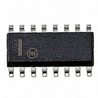
NE570D ON Semiconductor, NE570D Datasheet - Page 4

NE570D
Manufacturer Part Number
NE570D
Description
IC COMPANDOR DUAL GAIN 16-SOIC
Manufacturer
ON Semiconductor
Type
Compandorr
Datasheet
1.NE570DR2G.pdf
(10 pages)
Specifications of NE570D
Applications
Cellular Radio, Players
Mounting Type
Surface Mount
Package / Case
16-SOIC (0.300", 7.5mm Width)
Lead Free Status / RoHS Status
Contains lead / RoHS non-compliant
Available stocks
Company
Part Number
Manufacturer
Quantity
Price
Part Number:
NE570D
Manufacturer:
NXP/恩智浦
Quantity:
20 000
Part Number:
NE570DG
Manufacturer:
ON/安森美
Quantity:
20 000
Part Number:
NE570DR2G
Manufacturer:
ON/安森美
Quantity:
20 000
INTRODUCTION
electronic gain control circuits. For non−critical applications,
an integrated circuit operational transconductance amplifier
can be used, but when high−performance is required, one has
to resort to complex discrete circuitry with many expensive,
well−matched components. This paper describes an
inexpensive integrated circuit, the NE570 Compandor, which
offers a pair of high performance gain control circuits
featuring low distortion (<0.1 %), high signal−to−noise ratio
(90 dB), and wide dynamic range (110 dB).
CIRCUIT BACKGROUND
the requirements of the telephone system. When several
telephone channels are multiplexed onto a common line, the
resulting signal−to−noise ratio is poor and companding is
used to allow a wider dynamic range to be passed through the
channel. Figure 4 graphically shows what a compandor can
do for the signal−to−noise ratio of a restricted dynamic range
channel. The input level range of +20 dB to −80 dB is shown
undergoing a 2−to−1 compression where a 2.0 dB input level
change is compressed into a 1.0 dB output level change by the
compressor. The original 100 dB of dynamic range is thus
compressed to a 50 dB range for transmission through a
restricted dynamic range channel. A complementary
expansion on the receiving end restores the original signal
levels and reduces the channel noise by as much as 45 dB.
Much interest has been expressed in high performance
The NE570 Compandor was originally designed to satisfy
V
V
1
2
2.2 mF
2.2 mF
3, 14
2, 15
V
CC
20 kW
10 kW
Figure 3. Typical Test Circuit
= 15 V
13
4
http://onsemi.com
0.1 mF
DG
1, 16
NE570
2.2 mF
4
the rectifier and the gain control element. The phone system
requires a simple full−wave averaging rectifier with good
accuracy, since the rectifier accuracy determines the (input)
output level tracking accuracy. The gain cell determines the
distortion and noise characteristics, and the phone system
specifications here are very loose. These specs could have
been met with a simple operational transconductance
multiplier, or OTA, but the gain of an OTA is proportional
to temperature and this is very undesirable. Therefore, a
linearized transconductance multiplier was designed which
is insensitive to temperature and offers low noise and low
distortion performance. These features make the circuit
useful in audio and data systems as well as in
telecommunications systems.
The significant circuits in a compressor or expander are
8.2 kW
5, 12
LEVEL
INPUT
20 kW
30 kW
Figure 4. Restricted Dynamic Range Channel
0 dB
−
+
+20
−40
−80
10 mF
V
REF
8, 9
200 pF
7, 10
6, 11
NOISE
V
O
OUTPUT
LEVEL
−20
0 dB
−40
−80


