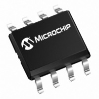
MCP6562-E/MS Microchip Technology, MCP6562-E/MS Datasheet - Page 17

MCP6562-E/MS
Manufacturer Part Number
MCP6562-E/MS
Description
IC COMP DUAL 1.8V PP 8-MSOP
Manufacturer
Microchip Technology
Type
General Purposer
Specifications of MCP6562-E/MS
Package / Case
8-TSSOP, 8-MSOP (0.118", 3.00mm Width)
Number Of Elements
2
Output Type
CMOS, Push-Pull, Rail-to-Rail, TTL
Voltage - Supply
1.8 V ~ 5.5 V
Mounting Type
Surface Mount
Mounting Style
SMD/SMT
Comparator Type
Low Power
No. Of Comparators
2
Response Time
47ns
Ic Output Type
CMOS, Push Pull, TTL
Supply Current
100µA
Supply Voltage Range
1.8V To 5.5V
Amplifier Case Style
MSOP
No. Of Pins
8
Rohs Compliant
Yes
Output Compatibility
CMOS, TTL
Lead Free Status / RoHS Status
Lead free / RoHS Compliant
Available stocks
Company
Part Number
Manufacturer
Quantity
Price
Part Number:
MCP6562-E/MS
Manufacturer:
MICROCHIP/微芯
Quantity:
20 000
4.3.2
Figure 4-6
using three resistors. The resulting hysteresis diagram
is shown in
FIGURE 4-6:
Hysteresis.
FIGURE 4-7:
Inverting Circuit.
In order to determine the trip voltages (V
for the circuit shown in
simplified to the Thevenin equivalent circuit with
respect to V
FIGURE 4-8:
© 2009 Microchip Technology Inc.
V
V
V
V
OH
DD
OL
SS
V
V
23
V
SS
IN
R
R
Low-to-High
V
2
3
shows an inverting circuit for single-supply
V
OUT
INVERTING CIRCUIT
Figure
DD
DD
, as shown in
R
23
4-7.
V
MCP656X
TLH
Inverting Circuit With
Hysteresis Diagram for the
Thevenin Equivalent Circuit.
MCP656X
+
Figure
-
V
DD
V
V
THL
Figure
DD
R
4-6, R
V
F
High-to-Low
R
SS
F
4-8.
2
and R
THL
V
V
DD
OUT
and V
V
3
OUT
can be
V
IN
TLH
)
Where:
Using this simplified circuit, the trip voltage can be
calculated using the following equation:
EQUATION 4-2:
Figure
typical values for V
4.4
With this family of comparators, the power supply pin
(V
capacitor (i.e., 0.01 µF to 0.1 µF) within 2 mm for good
edge rate performance.
4.5
Reasonable capacitive loads (e.g., logic gates) have
little impact on propagation delay (see
The supply current increases with increasing toggle
frequency
capacitive loads. The output slew rate and propagation
delay performance will be reduced with higher
capacitive loads.
Where:
DD
MCP6561/1R/1U/2/4
V
V
TLH
THL
for single supply) should have a local bypass
V
V
2-20, and
THL
TLH
Bypass Capacitors
Capacitive Loads
(Figure
=
=
=
=
V
V
R
V
OH
Figure 2-23
OL
23
23
OH
⎛
⎜
⎝
⎛
⎜
⎝
trip voltage from low to high
trip voltage from high to low
2-19),
=
---------------------- -
R
=
---------------------- -
R
23
23
and V
------------------ -
R
R
------------------ -
R
R
+
R
+
23
2
2
23
R
2
+
+
R F
R F
R
3
OL
R
3
R
especially
can be used to determine
⎞
⎟
⎠
⎞
⎟
⎠
3
3
.
+
+
×
V
V
V
23
DD
23
⎛
⎝
DS22139B-page 17
⎛
⎝
--------------------- -
R
--------------------- -
R
23
23
R
R
+
Figure
with
+
F
F
R
R
F
F
⎞
⎠
⎞
⎠
higher
2-31).


