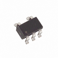
MAX919EUK+T Maxim Integrated Products, MAX919EUK+T Datasheet - Page 12

MAX919EUK+T
Manufacturer Part Number
MAX919EUK+T
Description
IC COMPARATOR BTR SOT23-5
Manufacturer
Maxim Integrated Products
Series
Beyond-the-Rails™r
Type
General Purposer
Datasheet
1.MAX920EUKT.pdf
(15 pages)
Specifications of MAX919EUK+T
Number Of Elements
1
Output Type
CMOS, Push-Pull, Rail-to-Rail, TTL
Voltage - Supply
1.8 V ~ 5.5 V
Mounting Type
Surface Mount
Package / Case
SC-74A, SOT-753
Number Of Channels
1 Channel
Product
Analog Comparators
Offset Voltage (max)
10 mV
Input Bias Current (max)
2 nA
Supply Voltage (max)
5.5 V
Supply Voltage (min)
1.8 V
Supply Current (max)
0.8 uA
Maximum Power Dissipation
571 mW
Maximum Operating Temperature
+ 85 C
Mounting Style
SMD/SMT
Minimum Operating Temperature
- 40 C
Comparator Type
General Purpose
No. Of Comparators
1
Response Time
22µs
Ic Output Type
CMOS, Push Pull
Supply Current
450nA
Supply Voltage Range
1.8V To 5.5V
Amplifier Case Style
SOT-23
Rohs Compliant
Yes
Lead Free Status / RoHS Status
Lead free / RoHS Compliant
Other names
MAX919EUK+T
MAX919EUK+TTR
MAX919EUK+TTR
SOT23, 1.8V, Nanopower, Beyond-the-Rails
Comparators With/Without Reference
6) Verify the trip voltages and hysteresis as follows:
Power-supply bypass capacitors are not typically
needed, but use 100nF bypass capacitors close to the
device’s supply pins when supply impedance is high,
supply leads are long, or excessive noise is expected
on the supply lines. Minimize signal trace lengths to
reduce stray capacitance. A ground plane and sur-
face-mount components are recommended.
Figure 4. MAX918/MAX920 Additional Hysteresis
12
=
V
IN
( ) ARE FOR MAX917/MAX918.
V
______________________________________________________________________________________
REF
V rising : V
V falling : V
IN
IN
Pin Configurations (continued)
R1
×
TOP VIEW
R1
IN- (REF)
Hysteresis = V
N.C.
⎛
⎜
⎝
R2
IN+
V
R1
EE
THR
THF
1
V
REF
Board Layout and Bypassing
1
2
4
3
+
=
=
R2
R3
1
V
REF
+
MAX917
MAX918
MAX919
MAX920
V
V
V
R3 R4
CC
EE
SO
CC
×
MAX918
MAX920
THR
1
+
R1
OUT
- V
⎞
⎟ −
⎠
⎛
⎜
⎝
6
R1
8
7
5
THF
1
R3 R4
N.C.
V
OUT
N.C.
+
CC
R1
+
R2
R4
1
+
R3
×
1
⎞
⎟
⎠
V
CC
Figure 5 shows a zero-crossing detector application.
The MAX919’s inverting input is connected to ground,
and its noninverting input is connected to a 100mV
signal source. As the signal at the noninverting input
crosses 0V, the comparator’s output changes state.
The Typical Application Circuit shows an application
that converts 5V logic to 3V logic levels. The MAX920 is
powered by the +5V supply voltage, and the pullup
resistor for the MAX920’s open-drain output is connect-
ed to the +3V supply voltage. This configuration allows
the full 5V logic swing without creating overvoltage on
the 3V logic inputs. For 3V to 5V logic-level translations,
simply connect the +3V supply voltage to V
+5V supply voltage to the pullup resistor.
Figure 5. Zero-Crossing Detector
100mV
5V (3V) LOGIC IN
100kΩ
100kΩ
P-P
Typical Application Circuit
IN-
IN+
IN+
IN-
+5V (+3V)
Zero-Crossing Detector
V
Logic-Level Translator
V
CC
EE
V
V
V
CC
CC
EE
LOGIC-LEVEL
TRANSLATOR
MAX920
MAX919
OUT
OUT
+3V (+5V)
CC
R
PULLUP
3V (5V)
LOGIC OUT
and the
P-P


