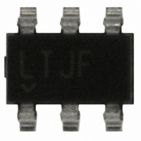
LT1719IS6#TRMPBF Linear Technology, LT1719IS6#TRMPBF Datasheet - Page 3

LT1719IS6#TRMPBF
Manufacturer Part Number
LT1719IS6#TRMPBF
Description
IC COMP R-RINOUT SINGLE SOT23-6
Manufacturer
Linear Technology
Series
UltraFast™r
Type
General Purposer
Specifications of LT1719IS6#TRMPBF
Number Of Elements
1
Output Type
CMOS, Rail-to-Rail, TTL
Voltage - Supply
2.7 V ~ 6 V
Mounting Type
Surface Mount
Package / Case
SOT-23-6
Comparator Type
General Purpose
No. Of Comparators
1
Response Time
4.5ns
Ic Output Type
CMOS, TTL
Output Compatibility
CMOS, TTL
Supply Current
4.6mA
Supply Voltage Range
2.7V To 6V
Rohs Compliant
Yes
Lead Free Status / RoHS Status
Lead free / RoHS Compliant
Other names
LT1719IS6#TRMPBFTR
Available stocks
Company
Part Number
Manufacturer
Quantity
Price
range, otherwise specifications are at T
V
SYMBOL PARAMETER
V
t
t
t
t
t
t
f
t
t
I
I
I
I
I
I
I
I
I
I
I
I
I
I
Note 1: Absolute Maximum Ratings are those values beyond which the
life of a device may be impaired.
Note 2: If one input is within these common mode limits, the other
input can go outside the common mode limits and the output will be
valid.
Note 3: The LT1719 comparator includes internal hysteresis. The trip
points are the input voltage needed to change the output state in each
direction. The offset voltage is defined as the average of V
V
Note 4: The LT1719S8 common mode rejection ratio is measured with
V
measured from V
ELECTRICAL CHARACTERISTICS
PD20
PD5
SKEW
JITTER
MAX
OFF
ON
CC
EE
S
+
SHDN5
SHDN3
CCS
SS
EES
+
CCSO
SSO
EEO
+
r
f
CC
OL
TRIP
CC
S
O
= 5V, V
= +V
–
, while the hysteresis voltage is the difference of these two.
S
Output Low Voltage
Propagation Delay
Propagation Delay
Propagation Delay Skew
Output Rise Time
Output Fall Time
Output Timing Jitter
Maximum Toggle Frequency
Turn-Off Delay
Wake-Up Delay
Positive Input Stage Supply Current
Negative Input Stage Supply Current
Positive Output Stage Supply Current
Supply Current
Shutdown Pin Current
Shutdown Pin Current
Disabled Supply Currents (LT1719S8) + V
= 5V and V
EE
= – 5V and is defined as the change in offset voltage
CM
= – 5.1V to V
EE
= –5V, for the LT1719S6 V
(LT1719S8 0nly) + V
(LT1719S8 0nly) + V
(LT1719S8 0nly) V
CM
(LT1719S6) V
(LT1719S8) V
(LT1719S8)
(LT1719S6) V
(LT1719S8) + V
(LT1719S8) Shutdown Pin Open
(LT1719S8)
(LT1719S6) V
= 3.8V, divided by 8.9V.
A
= 25 C. V
CONDITIONS
I
V
V
V
(Note 11)
10% to 90%
90% to 10%
V
f = 20MHz
V
V
Time to Z
Time to V
+ V
+ V
+ V
V
+V
+V
SINK
OVERDRIVE
OVERDRIVE
OVERDRIVE
IN
OVERDRIVE
OVERDRIVE
S
+
+
SHDN
+
+
S
S
S
S
S
S
S
= 5V
= 3V
S
= 6V, V
S
= 6V, Shutdown Pin Open
= V
= 1.2V
or V
or V
= V
= V
= V
= V
= V
= 6V, V
= 6V, V
= 10mA, V
+
CC
CM
= +V
= 5V, V
CC
CC
CC
CC
CC
+
+
TRIP
OUT
= 3V, V
OH
= 5V
= 3V
= 1V, V
P-P
SHDN
= 5V, V
= 3V, V
= 5V, V
= 3V, V
= 5V, V
S
= 20mV (Note 9)
= 20mV, V
= 5mV (Notes 9, 10) V
= 50mV, +V
= 50mV, +V
CC
CC
or V
– 0.5V
+
(6dBm), Z
= 5V, V
= 5V, V
and
10k
The
–
IN
= +V
EE
OL
= 0V, unless otherwise specified.
EE
EE
EE
EE
EE
= V
SHDN
, I
= 0V
S
= – 5V
= 0V
= – 5V
= 0V
= – 5V
LOAD
TRIP
– 0.5V
EE
EE
EE
denotes specifications that apply over the full operating temperature
S
S
IN
= 0.5V, V
= – 5V
= – 5V
= – 5V
or V
or V
–
= 1mA
= 50
– 10mV
Note 5: The LT1719S6 common mode rejection ratio is measured
with V
from V
Note 6: The LT1719S8 power supply rejection ratio is measured with
V
from V
voltage from V
divided by 3.3V.
Note 7: The 1719S6 power supply rejection ratio is measured with
V
V
+
+
CM
CM
+
= 3V
= 5V
= 2.7V to V
= 1V and is defined as the worst of: the change in offset voltage
= 1V and is defined as the change in offset voltage measured from
V
V
V
EE
EE
+
OVERDRIVE
CM
EE
–
–
= 5V and is defined as the change in offset voltage measured
(LT1719S8 only)
= 0V(LT1719S8)
= 0V(LT1719S6)
= 0V(LT1719S8)
= 0V(LT1719S6)
= – 5.5V to V
= –0.1V to V
+
CC
= 6V, divided by 3.3V.
= 20mV, C
= + V
t
t
PD
PD
EE
S
CM
+
–
= 2.7V to V
= 0V divided by 5.5V, or the change in offset
= 3.8V, divided by 3.9V.
OUT
= 10pF and for the LT1719S8
–300
–200
– 4.8
– 3.8
MIN
– 30
– 20
CC
= + V
–110
S
– 2.6
– 2.2
– 0.2
62.5
TYP
350
–80
4.5
4.2
0.5
2.5
2.2
1.0
0.9
4.2
3.3
4.6
4.2
0.2
0.1
0.1
0.1
0.2
15
11
70
75
= 6V (with V
7
7
7
MAX
–30
–20
0.4
6.5
8.0
1.5
2.2
1.8
10
13
30
50
80
20
20
40
8
6
9
7
LT1719
EE
= 0V)
UNITS
ps
ps
3
MHz
MHz
RMS
RMS
mA
mA
mA
mA
mA
mA
mA
mA
ns
ns
ns
ns
ns
ns
ns
ns
ns
ns
V
A
A
A
A
A
A
A
A
A
A


