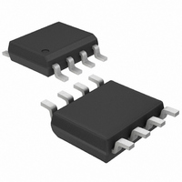
MAX982ESA+ Maxim Integrated Products, MAX982ESA+ Datasheet - Page 11

MAX982ESA+
Manufacturer Part Number
MAX982ESA+
Description
IC COMPARATOR OD 8-SOIC
Manufacturer
Maxim Integrated Products
Type
with Voltage Referencer
Datasheet
1.MAX983EPA.pdf
(17 pages)
Specifications of MAX982ESA+
Number Of Elements
2
Output Type
Open Drain
Voltage - Supply
2.5 V ~ 11 V, ±1.25 V ~ 5.5 V
Mounting Type
Surface Mount
Package / Case
8-SOIC (0.154", 3.90mm Width)
Number Of Channels
2 Channels
Product
Analog Comparators
Offset Voltage (max)
+/- 10 mV
Supply Voltage (max)
11 V
Supply Voltage (min)
2.5 V
Supply Current (max)
4.5 uA
Maximum Power Dissipation
471 mW
Maximum Operating Temperature
+ 85 C
Mounting Style
SMD/SMT
Minimum Operating Temperature
- 40 C
Comparator Type
General Purpose
No. Of Comparators
2
Response Time
12µs
Ic Output Type
CMOS, MOS, Open-Collector / Drain, TTL
Supply Current
3.1µA
Supply Voltage Range
± 1.25V To ± 5.5V
Rohs Compliant
Yes
Lead Free Status / RoHS Status
Lead free / RoHS Compliant
Hysteresis increases the comparators’ noise margin by
increasing the upper threshold and decreasing the
lower threshold (Figure 2).
To add hysteresis to the MAX9_1, MAX982, or MAX9_3,
connect resistor R1 between REF and HYST, and
connect resistor R2 between HYST and V- (Figure 3). If
no hysteresis is required, connect HYST to REF. When
hysteresis is added, the upper threshold increases by
the same amount that the lower threshold decreases.
The hysteresis band (the difference between the upper
and lower thresholds, V
twice the voltage between REF and HYST. The HYST
input can be adjusted to a maximum voltage of REF
and to a minimum voltage of (REF - 50mV). The
maximum difference between REF and HYST (50mV)
will therefore produce a 100mV (max) hysteresis band.
Use the following equations to determine R1 and R2:
where I
should not exceed the REF source capability, and
should be significantly larger than the HYST input
current. I
appropriate. If 2.4M
the equation for R1 and V
When hysteresis is obtained in this manner for the
MAX982/MAX9_3, the same hysteresis applies to both
comparators.
Hysteresis can be implemented with any comparator
using positive feedback, as shown in Figure 4. This
approach generally draws more current than circuits
using the HYST pin on the MAX9_1/MAX982/MAX9_3,
and the high feedback impedance slows hysteresis. In
addition, because the output does not source current,
any increase in the upper threshold is dependent on
the load or pullup resistor on the output.
__________Applications Information
REF
REF
(the current sourced by the reference)
values between 0.1µA and 4µA are usually
Hysteresis (MAX9_1/MAX982/MAX9_3)
R1 =
R2 =
R1 (k ) = V
______________________________________________________________________________________
is chosen for R2 (I
2
1.182 –
Hysteresis (MAX972/MAX9_4)
HB
HB
V
) is approximately equal to
HB
can be approximated as:
I
HB
I
REF
REF
(mV)
V
HB
2
Single/Dual-Supply Comparators
Hysteresis
REF
Ultra-Low-Power, Open-Drain,
= 0.5µA),
Power-supply bypass capacitors are not needed if the
supply impedance is low, but 100nF bypass capacitors
should be used when the supply impedance is high or
when the supply leads are long. Minimize signal lead
lengths to reduce stray capacitance between the input
and output that might cause instability. Do not bypass
the reference output.
The MAX9_3 is ideal for making window detectors
(undervoltage/overvoltage detectors). The schematic is
shown in Figure 5, with component values selected for a
4.5V undervoltage threshold and a 5.5V overvoltage
threshold. Choose different thresholds by changing the
values of R1, R2, and R3. To prevent chatter at the
output when the supply voltage is close to a threshold,
hysteresis has been added using R4 and R5. Taken
alone, OUTA would provide an active-low undervoltage
indication, and OUTB would give an active-low
overvoltage indication. Wired-ORing the two outputs
provides an active-high, power-good signal.
The design procedure is as follows:
1) Choose the required hysteresis level and calculate
Figure 4. External Hysteresis
values for R4 and R5 according to the formulas in
the Hysteresis (MAX9_1/MAX982/MAX9_3) section.
In this example, ±5mV of hysteresis has been added
at the comparator input (V
that the hysteresis apparent at V
because of the input resistor divider.
V
IN
Board Layout and Bypassing
V
REF
R
MAX9_4
H
GND
H
V+
V+
V-
= V
Window Detector
OUT
HB
IN
/2). This means
will be larger
R
PULLUP
11


