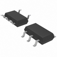
LT1716IS5#TRMPBF Linear Technology, LT1716IS5#TRMPBF Datasheet - Page 9

LT1716IS5#TRMPBF
Manufacturer Part Number
LT1716IS5#TRMPBF
Description
IC COMP OTT R-R 44V TSOT-23-5
Manufacturer
Linear Technology
Series
Over-The-Top®r
Type
General Purposer
Specifications of LT1716IS5#TRMPBF
Number Of Elements
1
Output Type
Push-Pull, Rail-to-Rail
Voltage - Supply
2.7 V ~ 44 V, ±1.35 V ~ 22 V
Mounting Type
Surface Mount
Package / Case
SOT-23-5 Thin, TSOT-23-5
Comparator Type
Precision
No. Of Comparators
1
Response Time
3µs
Ic Output Type
Pull Up
Supply Current
40µA
Supply Voltage Range
2.7V To 44V
Amplifier Case Style
SOT-23
No. Of Pins
5
Rohs Compliant
Yes
Lead Free Status / RoHS Status
Lead free / RoHS Compliant
Other names
LT1716IS5#TRMPBFTR
Available stocks
Company
Part Number
Manufacturer
Quantity
Price
APPLICATIONS INFORMATION
The LT1716 comparator features low power operation
with exceptional input precision with rail-to-rail input and
output swing. The comparator operates fl awlessly even
when the inputs are pulled over the positive rail or below
the negative rail.
Supply Voltage
The LT1716 operates from 2.7V to 44V. The comparator
can be shut down by removing V
input bias current is typically less than 3nA, even if the
inputs are 44V above the negative supply. The LT1716 is
protected against reverse battery voltages of up to 20V.
The reverse battery current is resistive as shown in the
Reverse Supply Current graph.
Inputs
The comparator inputs can swing from 0.5V above to 44V
above V
can be forced up to 5V below V
occuring at the output.
The LT1716 has three stages—NPN, PNP and common
base (see Simplifi ed Schematic)—resulting in three
distinct operating regions and two transition regions as
shown in the Input Bias Current vs Common Mode typical
performance curve.
For input voltages about 0.8V or more below V
input stage is active and the input bias current is typically
–4nA. The PNP differential input stage will have bias cur-
rent that fl ows out of the device. With a differential input
voltage of even just 100mV or so, there will be zero bias
current into the higher of the two inputs, while the current
fl owing out of the lower input will be twice the measured
bias current.
When the input voltage is about 0.5V or less from V
NPN state is operating and the input bias current is typically
10nA. Increases in temperature will cause the voltage at
which operation switches from the PNP stage to the NPN
stage to move towards V
NPN stage is untrimmed and is typically 500μV.
–
. If one input is within this range, the other input
+
. The input offset voltage of the
–
+
without phase reversal
. In this condition, the
+
, the PNP
+
, the
A Schottky diode in the collector of each NPN transistor
of the NPN input stage allows the LT1716 to operate with
either or both of its inputs above V
V
current is typically 4μA at room temperature. The input
offset voltage is typically 500μV when operating above
V
regardless of V
The transition to the negative common mode input stage
occurs at 0.3V above V
stage is active. When the inputs are 0.3V below V
common base input stage is active in addition to the PNP
stage. The input bias current out of each input becomes
V
input falls below the negative supply. Internal resistors
protect the inputs for faults below the negative supply of
up to 5V without phase reversal. The built-in 5k resistor
limits the current at each input to 1mA at 5V below the
negative supply. External matched input resistors can
be added for increased voltage fault operation below the
negative supply but the maximum input current should
be kept under 1mA.
Input Protection
The inverting and noninverting input pins of the LT1716
have on-chip protection. ESD protection is provided to
prevent damage during handling. The input transistors
have voltage clamping and limiting resistors to protect
against excursions as much as 5V below V
no clamping diodes between the inputs and the maximum
differential input voltage is 44V.
Output
The output stage of the LT1716 can drive loads connected
to a supply more positive than the device, the same as
comparators with open collector output stages. The
output of the LT1716 can be pulled up to 44V above V
regardless of V
+
+
IN
, the NPN transistor is fully saturated and the input bias
. The LT1716 will operate with its input 44V above V
/5kΩ. The LT1716 is designed to operate when either
+
+
.
.
–
. Above this trip point the PNP
+
. At about 0.3V above
LT1716
–
. There are
–
, the
1716fa
9
–
–
,
,


