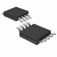
LT1711CMS8#TR Linear Technology, LT1711CMS8#TR Datasheet - Page 10

LT1711CMS8#TR
Manufacturer Part Number
LT1711CMS8#TR
Description
IC COMP R-RINOUT SINGLE 8-MSOP
Manufacturer
Linear Technology
Series
UltraFast™r
Type
General Purposer
Datasheet
1.LT1711CMS8PBF.pdf
(12 pages)
Specifications of LT1711CMS8#TR
Number Of Elements
1
Output Type
CMOS, Complementary, Rail-to-Rail, TTL
Voltage - Supply
2.4 V ~ 12 V, ±2.4 V ~ 6 V
Mounting Type
Surface Mount
Package / Case
8-TSSOP, 8-MSOP (0.118", 3.00mm Width)
Lead Free Status / RoHS Status
Contains lead / RoHS non-compliant
Other names
LT1711CMS8TR
Available stocks
Company
Part Number
Manufacturer
Quantity
Price
LT1711/LT1712
This comes out to 120
Thevenin equivalent source voltage is given by:
This amounts to an attenuation factor of 0.0978 with the
values shown. (The actual voltage on the lines will be cut
in half again due to the 120
attenuation factor is important is that it is the key to
deciding the ratio between the R2-R3 resistor divider in
the receiver path. This divider allows the receiver to reject
the large signal of the local transmitter and instead sense
the attenuated signal of the remote transmitter. Note that
in the above equations, R2 and R3 are not yet fully
determined because they only appear as a sum. This
allows the designer to now place an additional constraint
on their values. The R2-R3 divide ratio should be set to
equal half the attenuation factor mentioned above or:
Having already designed R2 + R3 to be 2.653k (by allocat-
ing input impedance across R
requisite 120 ), R2 and R3 then become 2529
123.5 respectively. The nearest 1% value for R2 is 2.55k
and that for R3 is 124 .
Voltage-Tunable Crystal Oscillator
The front page application is a variant of a basic crystal
oscillator that permits voltage tuning of the output fre-
quency. Such voltage-controlled crystal oscillators (VCXO)
10
TYPICAL APPLICATIO S
R3/R2 = 1/2 • 0.0976
V
TH
Figure 4. Performance of Figure 3’s Circuit When
Operated Unidirectionally. Eye is Wide Open
V
S
•
•
(
R
(
R
R
O
2
2
2
R
R
•
3
3
R
–
1
R
1
.
R
R
O
||(
1
1
)
)
for the values shown. The
R
O
2
, R1 and R2 + R3 to get the
U
R
Z
3
O
)
.) The reason this
171112 F04
and
are often employed where slight variation of a stable
carrier is required. This example is specifically intended to
provide a 4 NTSC sub-carrier tunable oscillator suitable
for phase locking.
The LT1711 is set up as a crystal oscillator. The varactor
diode is biased from the tuning input. The tuning network
is arranged so a 0V to 5V drive provides a reasonably
symmetric, broad tuning range around the 14.31818MHz
center frequency. The indicated selected capacitor sets
tuning bandwidth. It should be picked to complement loop
response in phase locking applications. Figure 6 is a plot
of tuning input voltage versus frequency deviation. Tuning
deviation from the 4 NTSC 14.31818MHz center fre-
quency exceeds 240ppm for a 0V to 5V input.
1
124 = 2.674k.
Using the design value of R2 + R3 = 2.653k rather than the implementation value of 2.55k +
Figure 5. Performance When Operated Simultaneous
Bidirectionally (Full Duplex). Crosstalk Appears as Noise.
Eye is Slightly Shut But Performance is Still Excellent
Figure 6. Control Voltage vs Output Frequency for the
Front Page Application Circuit. Tuning Deviation from
Center Frequency Exceeds 240ppm
9
8
7
6
5
4
3
2
1
0
0
14.31818MHz
14.3140MHz
1
INPUT VOLTAGE (V)
2
3
14.3217MHz
4
171112 F06
171112 F05
5


