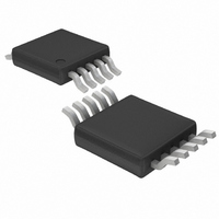
LT1715IMS Linear Technology, LT1715IMS Datasheet - Page 16

LT1715IMS
Manufacturer Part Number
LT1715IMS
Description
IC COMPARATOR 150MHZ DUAL 10MSOP
Manufacturer
Linear Technology
Series
UltraFast™r
Type
General Purposer
Datasheet
1.LT1715CMS.pdf
(20 pages)
Specifications of LT1715IMS
Number Of Elements
2
Output Type
CMOS, Rail-to-Rail, TTL
Voltage - Supply
2.7 V ~ 12 V
Mounting Type
Surface Mount
Package / Case
10-TFSOP, 10-MSOP (0.118", 3.00mm Width)
Lead Free Status / RoHS Status
Contains lead / RoHS non-compliant
Available stocks
Company
Part Number
Manufacturer
Quantity
Price
Company:
Part Number:
LT1715IMS
Manufacturer:
LT
Quantity:
10 000
Part Number:
LT1715IMS
Manufacturer:
LINEAR/凌特
Quantity:
20 000
Part Number:
LT1715IMS#PBF
Manufacturer:
LINEAR/凌特
Quantity:
20 000
Part Number:
LT1715IMS#TRPBF
Manufacturer:
LT/凌特
Quantity:
20 000
APPLICATIONS INFORMATION
LT1715
The bias conditions and signal swings in the output stage
are designed to turn their respective output transistors off
faster than on. This helps minimize the surge of current
from +V
the frequency-dependent increase in power consumption.
The frequency dependence of the supply current is shown
in the Typical Performance Characteristics.
Speed Limits
The LT1715 comparator is intended for high speed ap-
plications, where it is important to understand a few
limitations. These limitations can roughly be divided into
three categories: input speed limits, output speed limits,
and internal speed limits.
There are no significant input speed limits except the shunt
capacitance of the input nodes. If the 2pF typical input
nodes are driven, the LT1715 will respond.
The output speed is constrained by three mechanisms, the
fi rst of which is the slew currents available from the output
transistors. To maintain low power quiescent operation,
the LT1715 output transistors are sized to deliver 35mA
to 60mA typical slew currents. This is sufficient to drive
small capacitive loads and logic gate inputs at extremely
high speeds. But the slew rate will slow dramatically with
heavy capacitive loads. Because the propagation delay (t
definition ends at the time the output voltage is halfway
between the supplies, the fixed slew current makes the
LT1715 faster at 3V than 5V with large capacitive loads
and suffi cient input overdrive.
Another manifestation of this output speed limit is skew,
the difference between t
of the LT1715 vary with the process variations of the PNP
and NPN transistors, for rising edges and falling edges
respectively. The typical 0.5ns skew can have either polar-
ity, rising edge or falling edge faster. Again, the skew will
increase dramatically with heavy capacitive loads.
A fi nal limit to output speed is the turn-on and turn-off
time of the output devices. Each device has substantial
16
S
to ground that occurs at transitions, to minimize
PD
+
and t
PD
–
. The slew currents
PD
)
base charge that requires one nanosecond or more of
active charging or discharging by the bias current of
the Darlington driver stage. When toggle rates are high
enough that insuffi cient time is allowed for this turn-on
or turn-off, glitches may occur leading to dropout or runt
pulses. Furthermore, power consumption may increase
nonlinearly if devices are not turned off before the oppos-
ing cycle. However, once the toggle frequency increases
or decreases, the part will easily leave this undesired
operating mode no worse for the wear provided there
is adequate heat sinking toprevent thermal overload. At
frequencies well beyond the maximum toggle rate, the part
will toggle with limited output swing and well controlled
power consumption.
The internal speed limits manifest themselves as disper-
sion. All comparators have some degree of dispersion,
defined as a change in propagation delay versus input
overdrive. The propagation delay of the LT1715 will vary
with overdrive, from a typical of 4ns at 20mV overdrive
to 6ns at 5mV overdrive (typical). The LT1715’s primary
source of dispersion is the hysteresis stage. As a change
of polarity arrives at the gain stage, the positive feedback
of the hysteresis stage subtracts from the overdrive avail-
able. Only when enough time has elapsed for a signal to
propagate forward through the gain stage, backwards
through the hysteresis path and forward through the gain
stage again, will the output stage receive the same level
of overdrive that it would have received in the absence of
hysteresis.
The LT1715 is several hundred picoseconds faster when
V
to the internal speed limit; the gain stage operates between
V
bias due to reduced silicon junction capacitances.
In many applications, as shown in the following examples,
there is plenty of input overdrive. Even in applications pro-
viding low levels of overdrive, the LT1715 is fast enough
that the absolute dispersion of 2ns (= 6 – 4) is often small
enough to ignore.
EE
EE
= –5V, relative to single supply operation. This is due
and +V
S
, and it is faster with higher reverse voltage
1715fa


