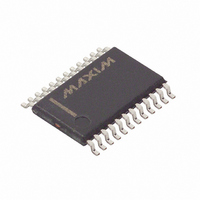
MAX9602EUG+ Maxim Integrated Products, MAX9602EUG+ Datasheet - Page 4

MAX9602EUG+
Manufacturer Part Number
MAX9602EUG+
Description
IC COMPARATOR HS 24-TSSOP
Manufacturer
Maxim Integrated Products
Type
General Purposer
Datasheet
1.MAX9600EUP.pdf
(12 pages)
Specifications of MAX9602EUG+
Number Of Elements
4
Output Type
Complementary, Differential, PECL
Mounting Type
Surface Mount
Package / Case
24-TSSOP
Number Of Channels
4 Channels
Product
Digital Comparators
Offset Voltage (max)
+/- 9 mV
Input Bias Current (max)
20 uA
Supply Voltage (max)
5 V
Supply Voltage (min)
1 V
Supply Current (max)
10000 uA
Maximum Power Dissipation
975 mW
Maximum Operating Temperature
+ 85 C
Mounting Style
SMD/SMT
Minimum Operating Temperature
- 40 C
Comparator Type
High Speed
No. Of Comparators
4
Response Time
500ps
Ic Output Type
Differential, PECL
Supply Current
28mA
Supply Voltage Range
4.3V To 6.3V, -4V To -6V
Rohs Compliant
Yes
Lead Free Status / RoHS Status
Lead free / RoHS Compliant
Dual ECL and Dual/Quad PECL, 500ps,
Ultra-High-Speed Comparators
AC ELECTRICAL CHARACTERISTICS
(V
GND = 0V, R
T
Note 1: All devices are 100% production tested at T
Note 2: Does not include output state current in Q_, Q_.
Note 3: Guaranteed by design.
Note 4: Propagation delay skew (t
Note 5: Propagation delay match is the difference of t
Note 6: Latch setup and hold-timing specifications are for a differentially driven latch signal.
4
A
Tracking Frequency Toggle Rate
Minimum Pulse Width
Propagation Delay
Propagation Delay Tempco
Propagation Delay Skew
Propagation Delay Match
Propagation Delay Dispersion
Overdrive
Propagation Delay Dispersion
Common-Mode Voltage
Propagation Delay Dispersion
Input Slew Rate
Propagation Delay Dispersion
Duty Cycle
Propagation Delay Dispersion
Pulse Width
Unit-to-Unit Propagation Delay
Match
Output Jitter
Input Capacitance
Latch Setup Time
Latch Hold Time
Minimum Pulse Width
Latch to Output Delay
Rise Time and Fall Time
CC
= +25°C, unless otherwise noted.) (Note 1)
_______________________________________________________________________________________
= 5V, V
to-low output transition vs. the low-to-high output transition.
PARAMETER
L
EE
= 50Ω to -2V (MAX9600), V
= -5.2V, V
CM
= 0V, HYS_ = open (MAX9600/MAX9601), LE_ = low, LE_ = high (MAX9600/MAX9601), C
PDSKEW
SYMBOL
t
t
PD-,
PDSKEW
TCt
f
t
t
t
MAX
t
C
LPW
R,
t
LPD
t
PW
LS
LH
IN
t
PD
CCO
t
PD+
) is for a single channel and is the difference between the propagation delay to the high-
F
_ = 5V, R
V
V
Input overdrive = 100mV, Figure 1, (Note 3)
Input overdrive = 100mV (Note 4)
Input overdrive = 100mV (Note 5)
10mV to 100mV
100mV to 2V
V
input
overdrive =
100mV
Input overdrive = 100mV
V
IN_+ or IN_, with respect to GND
Figure 1, (Notes 3, 6)
Figure 1, (Notes 3, 6)
Figure 1
Figure 1
20% to 80%, Figure 1
OUT
OUT
IN
IN
= 2V
PD-
= 1V
A
= 550mV
= 550mV
= +25°C. Specifications over temperature are guaranteed by design.
L
or t
P-P
P-P
= 50Ω to 3V (MAX9601/MAX9602), T
PD+
; 50MHz
P-P
P-P
of one channel to the t
(V
0.2V/ns to 10V/ns
10% to 90% at 250MHz
350ps to 1ns
CONDITIONS
EE
, input overdrive = 100mV
, input overdrive = 100mV
+ 3V) ≤ V
CM
≤ (V
PD-
CC
or t
- 2V)
PD+
A
of another channel of the same device.
= T
MIN
250
300
MIN
to T
MAX
TYP
250
500
300
250
200
200
0.5
10
40
15
40
10
40
30
20
50
80
85
4
2
. Typical values are at
MAX
700
L
UNITS
Gbps
ps/°C
= 5pF,
pF
ps
ps
ps
ps
ps
ps
ps
ps
ps
ps
ps
ps
fs


