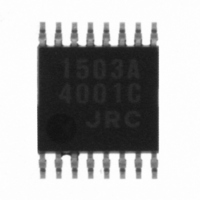
NJM2285V-TE2# NJR, NJM2285V-TE2# Datasheet

NJM2285V-TE2#
Specifications of NJM2285V-TE2#
NJM#2285V-TE2
Related parts for NJM2285V-TE2#
NJM2285V-TE2# Summary of contents
Page 1
... Wide Bandwidth Frequency Feature 10MHz (2V • Package Outline DIP16, DMP16, SSOP16 • Bipolar Technology ■ APPLICATIONS • VCR, Video Camera, AV-TV, Video Disk Player. ■ BLOCK DIAGRAM Ver.2004-02-17 ■ PACKAGE OUTLINE (4.75 to 13.0V) Input) P-P NJM2285D NJM2285M NJM2285V NJM2285D NJM2285M NJM2285V - 1 - ...
Page 2
MAXIMUM RATINGS PARAMETER Supply Voltage Power Dissipation Operating Temperature Range Storage Temperature Range ■ ELECTRICAL CHARACTERISTICS PARAMETER SYMBOL Operating Current (1) Operating Current (2) Voltage Gain Frequency Gain Differential Gain Differential Phasa Output Offset Voltage Crosstalk Switch Change Over ...
Page 3
TERMINLAL EXPLANATION PIN No. PIN NAME [Input [Input] 2 CTL 1 12 CTL 2 7 ...
Page 4
TEST CIRCUIT This IC requires 1MΩ resistance between INPUT and GND pin for clamp type input since the minute current causes an unstable pin voltage. Parameter CC1 CC2 ...
Page 5
TYPICAL CHARACTERISTICS Operating Current 1 vs. Temperature Voltage Gain 1 vs. Temperature Differential Gain 1 vs. Temperature Ver.2004-02-17 Operating Current 2 vs. Temperature Frequency Gain 1 vs. Temperature Differential Phase 1 vs. Temperature - 5 - ...
Page 6
TYPICAL CHARACTERISTICS Offset Voltage 1 vs. Temperature Crosstalk 2 vs. Temperature Crosstalk 4 vs. Temperature - 6 - Crosstalk 1 vs. Temperature Crosstalk 3 vs. Temperature Crosstalk 5 vs. Temperature Ver.2004-02-17 ...
Page 7
TYPICAL CHARACTERISTICS Crosstalk 6 vs. Temperature Supply Current 1 vs. Operating Voltage Frequency vs. Operating Voltage Ver.2004-02-17 Switch Change Over 1 vs. Temperature Voltage Gain 1 vs. Operating Voltage Differential Gain 1 vs. Operating Voltage - 7 - ...
Page 8
TYPICAL CHARACTERISTICS Differential Phase 1 vs. Operating Voltage Crosstalk 1 vs. Operating Voltage Crosstalk 3 vs. Operating Voltage - 8 - Offset Voltage 1 vs. Operating Voltage Crosstalk 2 vs. Operating Voltage Crosstalk 4 vs. Operating Voltage Ver.2004-02-17 ...
Page 9
TYPICAL CHARACTERISTICS Crosstalk 5 vs. Operating Voltage V Switch Change Over 1 vs. Operating Voltage Differential Gain 1 vs. Load Resistor Ver.2004-02-17 + (V) Crosstalk 6 vs. Operating Voltage V Differential Gain 1 vs. Frequency Differential Gain 3 vs. ...
Page 10
TYPICAL CHARACTERISTICS Differential Phase 1 vs. Load Resistor Differential Gain 1 vs. APL Differential Phase 1 vs. APL - 10 - Differential Phase 3 vs. Load Resistor Differential Gain 3 vs. APL Differential Phase 3 vs. APL Ver.2004-02-17 ...
Page 11
TYPICAL CHARACTERISTICS Total Harmonic Distortion vs. Load Resistor Ver.2004-02- ...
Page 12
APPLICATION This IC requires 1MΩ resistance between INPUT and GND pin for clamp type input since the minute current causes an unstable pin voltage. This IC requires 0.1µF capacitor between INPUT and GND, 1MΩ resistance between INPUT and GND ...


