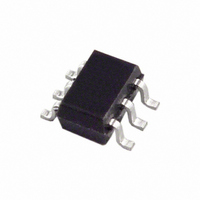
ADA4430-1YKSZ-R2 Analog Devices Inc, ADA4430-1YKSZ-R2 Datasheet - Page 5

ADA4430-1YKSZ-R2
Manufacturer Part Number
ADA4430-1YKSZ-R2
Description
IC FILTER VIDEO ULTRA LP SC70-6
Manufacturer
Analog Devices Inc
Type
Video Filterr
Datasheet
1.ADA4430-1YKSZ-RL.pdf
(20 pages)
Specifications of ADA4430-1YKSZ-R2
Design Resources
Reconstruction Video Filter Using ADA4430-1 Amplifier After ADV7393 Video Encoder (CN0101)
Applications
Cell Phones, Digital Cameras, Media Players
Mounting Type
Surface Mount
Package / Case
SC-70-6, SC-88, SOT-363
Ic Filter Type
Lowpass
Video Signal Filter
SD
Frequency
27MHz
Bandwidth
9.7MHz
Filter Order
6th
Supply Voltage Range
2.5V To 6V
Tv / Video Case Style
SC-70
No. Of Pins
6
Lead Free Status / RoHS Status
Lead free / RoHS Compliant
ABSOLUTE MAXIMUM RATINGS
Table 3.
Parameter
Supply Voltage
Power Dissipation
Storage Temperature Range
Operating Temperature Range
Lead Temperature (Soldering 10 sec)
Junction Temperature
Stresses above those listed under Absolute Maximum Ratings
may cause permanent damage to the device. This is a stress
rating only; functional operation of the device at these or any
other conditions above those indicated in the operational
section of this specification is not implied. Exposure to absolute
maximum rating conditions for extended periods may affect
device reliability.
THERMAL RESISTANCE
θ
specified for a device soldered in the circuit board.
Table 4. Thermal Resistance
Package Type
6-Lead SC70
6-Lead SOT-23
Maximum Power Dissipation
The maximum safe power dissipation in the ADA4430-1
package is limited by the associated rise in junction temperature
(T
transition temperature, the plastic changes its properties. Even
temporarily exceeding this temperature limit can change the
stresses that the package exerts on the die, permanently shifting
the parametric performance of the ADA4430-1. Exceeding a
junction temperature of 150°C for an extended period can
result in changes in the silicon devices, potentially causing
failure.
JA
J
) on the die. At approximately 150°C, which is the glass
is specified for the worst-case conditions, that is, θ
θ
430
170
JA
Rating
6 V
See Figure 3
−65°C to +125°C
−40°C to +125°C
300°C
150°C
JA
Unit
°C/W
°C/W
is
Rev. C | Page 5 of 20
The power dissipated in the package (P
quiescent power dissipation and the power dissipated in the
package due to the load drive. The quiescent power is the
voltage between the supply pins (V
current (I
upon the particular application. The power due to load drive is
calculated by multiplying the load current by the associated
voltage drop across the device. RMS voltages and currents must
be used in these calculations.
Airflow increases heat dissipation, effectively reducing θ
addition, more metal directly in contact with the package leads
from metal traces, through holes, ground, and power planes
reduces the θ
Figure 3 shows the maximum safe power dissipation in the
package vs. the ambient temperature for the 6-lead SC70
(430°C/W) and the 6-lead SOT-23 (170°C/W) on a JEDEC
standard 4-layer board.
ESD CAUTION
Figure 3. Maximum Power Dissipation vs. Temperature for a 4-Layer Board
1.2
1.0
0.8
0.6
0.4
0.2
0
–40
S
). The power dissipated due to the load drive depends
JA
.
–20
0
AMBIENT TEMPERATURE (°C)
20
SOT-23
SC70
40
S
) times the quiescent
60
D
) is the sum of the
80
ADA4430-1
100
JA
120
. In


