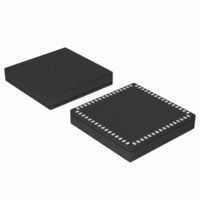
TDA18271HD/C2,557 NXP Semiconductors, TDA18271HD/C2,557 Datasheet - Page 17

TDA18271HD/C2,557
Manufacturer Part Number
TDA18271HD/C2,557
Description
IC TV SILICON TUNER 64-HLQFN
Manufacturer
NXP Semiconductors
Type
Silicon Tunerr
Specifications of TDA18271HD/C2,557
Applications
Set-Top Boxes
Mounting Type
Surface Mount
Package / Case
*
Lead Free Status / RoHS Status
Lead free / RoHS Compliant
Other names
935285058557
TDA18271HD/C2
TDA18271HD/C2
TDA18271HD/C2
TDA18271HD/C2
NXP Semiconductors
TDA18211HD_5
Product data sheet
9.3.10 Description of Cal Post-Divider byte
9.3.11 Description of Cal divider bytes 1, 2 and 3
9.3.9 Description of Easy Prog byte 5
The image rejection calibration consists in optimizing some tunable parameters inside the
mixer throughout a set of internal measurements, leading to ensure a 65 dB typical value
of image rejection. The internal signal used during this phase is generated by the PLL
calibration (CAL PLL).
The RF tracking filters central frequency can be adjusted with the tuning word
RFC_CPROG. The RF tracking filters calibration (RFCAL) consists of an internal tone at
the input of the tracking filters (with the CAL PLL), and finding the RFC_CPROG
corresponding to the maximum transmitted power. The RFCAL is just a little part of a
more complex algorithm fully described in the flowcharts in
The Power detection mode is a Normal mode where the detector used for the calibrations
is switched ON. This special mode enables to sense the power at the input of the
TDA18211HD and makes the power scan algorithm possible (see
“Flowchart
Table 18.
Legend: * power-on reset value
Table 19.
Legend: * power-on reset value
Table 20.
Legend: * power-on reset value
Bit
7
6 to 4 IR_GSTEP[2:0]
3
2 to 0 IR_MEAS[2:0]
Bit
7 to 0
Address Register Bit
09h
0Ah
0Bh
Symbol
EXTENDED_REG
-
Symbol
CAL_POST_DIV[7:0]
CD1
CD2
CD3
EP5 - Easy Prog byte 5 (subaddress 07h) bit description
CPD - Cal Post-Divider byte (subaddress 08h) bit description
CD1, CD2 and CD3 - Cal divider bytes 1, 2 and 3 (address 09h, 0Ah and 0Bh) bit
description
TDA18211PowerScan”).
7
6 to 0 CAL_DIV[22:16]
7 to 0 CAL_DIV[15:8]
7 to 0 CAL_DIV[7:0]
Rev. 05 — 2 June 2009
Access Value
R/W
R/W
R/W
R/W
Symbol
-
Access
R/W
1
0*
011*
0*
000*
Value
00h*
Description
enables the extended register addressing
gain step for image rejection calibration
must be set to logic 0
image rejection measurement frequency range
(see
Access Value Description
R/W
R/W
R/W
R/W
extended register (00h to 26h)
limited register (00h to 0Fh); only 1 byte can
be programmed after address 0Fh within 1
transmission
Table
Description
calibration synthesizer post-divider (see
Table
0*
00h*
00h*
00h*
51)
46)
Section
must be set to logic 0
calibration synthesizer main
divider bits
TDA18211HD
DVB-T Silicon Tuner IC
Section 9.4.8
9.4.
© NXP B.V. 2009. All rights reserved.
17 of 66


