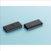
APU3146 Advanced Power Electronics Corp., APU3146 Datasheet - Page 9

APU3146
Manufacturer Part Number
APU3146
Description
The APU3046 IC combines a Dual synchronous Buck controller and a linear regulator controller, providing a cost-effective, high performance and flexible solution for multi-output applications
Manufacturer
Advanced Power Electronics Corp.
Datasheet
1.APU3146.pdf
(28 pages)
Specifications of APU3146
Vin(min)
0.8
Vin(max)
16
Vout(min)
0.8
Vout(max)
5
Iout(max)
30
Frequency
200~500KHz
Power Good
?
Package
28-Pin TSSOP ,28-Pin SOIC
Frequency Synchronization
The APU3146 is capable of accepting an external digital
synchronization signal. Synchronization will be enabled
by the rising edge at an external clock. Per-channel switch-
ing frequency is set by external resistor (Rt). The free
running oscillator frequency is twice the per-channel fre-
quency. During synchronization, Rt is selected such that
the free running frequency is 20% below the sync fre-
quency. Synchronization capability is provided for both 2-
output and 2-phase configurations. When unused, the
Sync pin will remain floating and is noise immune.
Thermal Shutdown
Temperature sensing is provided inside APU3146. The trip
threshold is typically set to 140 C. When trip threshold is
exceeded, thermal shutdown turns off both FETs. Ther-
mal shutdown is not latched and automatic restart is ini-
tiated when the sensed temperature drops to normal
range. There is a 20 C hysteresis in the shutdown thresh-
old.
Power Good
The APU3146 provides a power good signal. The power
good signal should be available after both outputs have
reached regulation. This pin needs to be externally pulled
high. High state indicates that outputs are in regulation.
Power good will be low if either one of the output voltages
is 10% below the set value. There is only one power good
for both outputs.
Over-Voltage Protection OVP
Over-voltage is sensed through separate V
Vsen1 and Vsen2. A separate OVP circuit is provided for
each output. Upon over-voltage condition of either one of
the outputs, the OVP forces a latched shutdown on both
outputs. In this mode, the upper FET drivers turn-off and
the lower FET drivers turn-on, thus crowbaring the out-
puts. Reset is performed by recycling either Vcc.
Error Amplifier
The APU3146 is a voltage mode controller. The error am-
plifiers are of transconductance type. In independent mode,
each amplifier closes the loop around its own output volt-
age. In current sharing mode, amplifier 1 becomes the
master which regulates the common output voltage. Am-
plifier 2 performs the current sharing function. Both am-
plifiers are capable of operating with Type III compensa-
tion control scheme.
Low Temperature Start-Up
The controller is capable of starting at -40 C ambient
temperature.
OUT
sense pins
Operation Frequency Selection
The optimum operating frequency range for APU3146 is
300KHz per phase, theoretically the APU3146 can be
operated at higher switching frequency (e.g. 500KHz).
However the power dissipation for IC, which is function
of applied voltage, gate drivers load and switching fre-
quency, will result in higher junction temperature of de-
vice. It may exceed absolute maximum rating of junc-
tion temperature, figure 18 (page 16) shows case tem-
perature versus switching frequency with different ca-
pacitive loads.
This should be considered when using APU3146 for such
application. The below equation shows the relationship
between IC's maximum power dissipation and Junction
temperature:
Where:
Tj: Maximum Operating Junction Temperature (125°C)
TA: Ambient Temperature (70°C)
θ
For Tj=125°C TA=70°C and θ
This will result to power dissipation of 650mW, this in-
cludes biasing current for all four external MOSFETs
and IC's biasing current.
The switching frequency is determined by an external
resistor (Rt). The switching frequency is approximately
inversely proportioned to resistance (see Fig 10).
Shutdown
The outputs can be shutdown independently by pulling
the respective soft-start pins below 0.3V. This can be
easily done by using an external small signal transis-
tor. During shutdown both MOSFETs will be turned off.
During this mode the LDO will stay on. Cycling soft-
start pins will clear all fault latches and normal opera-
tion will resume.
JA
Figure 10- Switching Frequency versus External Resistor.
= Thermal Impedance of package (84°C/W)
700
650
600
550
500
450
400
350
300
250
200
10
Per channel Switching Frequency vs. RT
Pd =
20
Τ
θ
J-
JA
Τ
A
RT(Kohm)
30
JA
=84°C/W
APU3146
40
50
9/28


