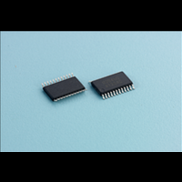
APU3046 Advanced Power Electronics Corp., APU3046 Datasheet - Page 4

APU3046
Manufacturer Part Number
APU3046
Description
The APU3046 IC combines a Dual synchronous Buck controller and a linear regulator controller, providing a
cost-effective, high performance and flexible solution for multi-output applications
Manufacturer
Advanced Power Electronics Corp.
Datasheet
1.APU3046.pdf
(19 pages)
Specifications of APU3046
Vin(min)
1.25
Vin(max)
25
Vout(min)
1.25
Vout(max)
5
Iout(max)
20
Frequency
200~400KHz
Power Good
?
Scp
?
Otp
?
Package
24-Pin TSSOP
APU3046
PIN#
BLOCK DIAGRAM
10,15
11,14
12
13
17
18
19
20
22
23
24
Comp2
Comp1
V
SEN33
Sync
V
Vp2
Fb1
Fb2
Fb3
Vcc
REF
PIN SYMBOL
HDrv2, HDrv1
SS
LDrv2, LDrv1
Rt
POR
VccLDO
21
7
2
19
PGood
22
20
5
8
1
3
6
4
PGnd
V
V
Gnd
Fb3
Fb2 Monitor Shut Down
V
SS
SEN33
OUT3
1.25V
1.25V
CL
10K
25K
25K
25K
25K
25K
25K
1.25V
25uA
Output driver for the high side power MOSFET. Connect a diode, such as BAT54 or 1N4148,
from these pins to ground for the application when the inductor current goes negative
(Source/Sink), soft-start at no load and for the fast load transient from full load to no load.
Output driver for the synchronous power MOSFET.
This pin serves as the separate ground for MOSFET’s driver and should be connected to
the system’s ground plane. A high frequency capacitor (0.1 to 1mF) must be connected
from Vcc, V
Supply voltage for the low side output drivers.
Separate input supply for LDO controller.
Driver signal for the LDO’s external transistor.
LDO’s feedback pin, connected to a resistor divider to set the output voltage of LDO.
This pin provides soft-start for the switching regulator. An internal current source charges
an external capacitor that is connected from this pin to ground which ramps up the output
of the switching regulator, preventing it from overshooting as well as limiting the input
current. The converter can be shutdown by pulling this pin below 0.5V.
Sense the LDO input voltage for UVLO.
Power good pin. This pin is a collector output that switches Low when any of the outputs
are outside of the specified under voltage trip point.
Analog ground for internal reference and control circuitry. Connect to PGnd with a short
trace.
PIN DESCRIPTION
Figure 2 - Block diagram of the APU3046.
CL
64uA Max
Error Amp1
Error Amp2
, VcH1 and VcH2 pins to this pin for noise free operation.
40mA LDO Controller
Fb1
Fb2
Fb3
VccLDO
Ramp1
Ramp2
Vsen33
VcH1
VcH2
PWM Comp1
PWM Comp2
4.2V / 4.0V
4.2V / 4.0V
2.5V / 2.3V
3.5V / 3.3V
3.5V / 3.3V
Two Phase
Oscillator
0.5V
PGood
Generator
Bias
Set1
Set2
UVLO
Reset Dom
Reset Dom
S
R
S
R
POR
Q
Q
3V
1.25V
POR
SS>2V
2V
SS
16
15
13
14
10
11
12
23
17
18
24
9
V
VcH1
HDrv1
V
LDrv1
VcH2
HDrv2
LDrv2
PGnd
PGood
VccLDO
Gnd
CL
OUT3
4/18


