74F125SCX Fairchild Semiconductor, 74F125SCX Datasheet - Page 2
74F125SCX
Manufacturer Part Number
74F125SCX
Description
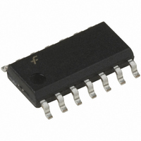
IC BUFFER TRI-ST QD N-INV 14SOIC
Manufacturer
Fairchild Semiconductor
Series
74Fr
Specifications of 74F125SCX
Logic Type
Buffer/Line Driver, Non-Inverting
Number Of Elements
4
Number Of Bits Per Element
1
Current - Output High, Low
15mA, 64mA
Voltage - Supply
4.5 V ~ 5.5 V
Operating Temperature
0°C ~ 70°C
Mounting Type
Surface Mount
Package / Case
14-SOIC (3.9mm Width), 14-SOL
Logic Family
F
Number Of Channels Per Chip
4
Polarity
Non-Inverting
Supply Voltage (max)
5.5 V
Supply Voltage (min)
4.5 V
Maximum Operating Temperature
+ 70 C
Mounting Style
SMD/SMT
High Level Output Current
- 15 mA
Low Level Output Current
64 mA
Minimum Operating Temperature
0 C
Number Of Lines (input / Output)
4 / 3
Output Type
3-State
Propagation Delay Time
7.5 ns at 5 V
Dc
9952
Lead Free Status / RoHS Status
Lead free / RoHS Compliant
Other names
74F125SCX
74F125SCXTR
74F125SCXTR
Available stocks
Company
Part Number
Manufacturer
Quantity
Price

Part Number:
74F125SCX
Manufacturer:
FAIRCHILD/仙童
Quantity:
20 000


www.fairchildsemi.com
V
V
V
V
V
I
I
I
I
I
I
I
I
I
I
I
t
t
t
t
t
t
IH
BVI
IL
OZH
OZL
OS
CEX
ZZ
CCH
CCL
CCZ
PLH
PHL
PZH
PZL
PHZ
PLZ
Absolute Maximum Ratings
DC Electrical Characteristics
AC Electrical Characteristics
IH
IL
CD
OH
OL
Symbol
Symbol
Storage Temperature
Ambient Temperature under Bias
Junction Temperature under Bias
V
Input Voltage (Note 2)
Input Current (Note 2)
Voltage Applied to Output
Current Applied to Output
CC
in HIGH State (with V
Standard Output
3-STATE Output
in LOW State (Max)
Pin Potential to Ground Pin
Input HIGH Voltage
Input LOW Voltage
Input Clamp Diode Voltage
Output HIGH
Voltage
Output LOW
Voltage
Input HIGH Current
Input HIGH Current
Breakdown Test
Input LOW Current
Output Leakage Current
Output Leakage Current
Output Short-Circuit Current
Output HIGH Leakage Current
Buss Drainage Test
Power Supply Current
Power Supply Current
Power Supply Current
Propagation Delay
Output Enable Time
Output Disable Time
Parameter
CC
Parameter
0V)
twice the rated I
10% V
10% V
10% V
5% V
5% V
30 mA to 5.0 mA
CC
CC
CC
CC
CC
65 C to 150 C
55 C to 125 C
55 C to 150 C
0.5V to 7.0V
0.5V to 7.0V
0.5V to 5.5V
(Note 1)
0.5V to V
Min
2.0
2.4
2.0
2.7
2.0
100
OL
(mA)
CC
18.5
31.7
27.6
Typ
2
Min
2.0
3.0
3.5
3.5
1.5
1.5
Recommended Operating
Conditions
Note 1: Absolute maximum ratings are values beyond which the device
may be damaged or have its useful life impaired. Functional operation
under these conditions is not implied.
Note 2: Either voltage limit or current limit is sufficient to protect inputs.
Free Air Ambient Temperature
Supply Voltage
V
T
C
CC
Max
0.55
24.0
40.0
35.0
A
100
250
500
L
0.8
20.0
20
50
225
1.2
50
Typ
4.0
4.6
4.7
5.3
3.9
4.0
50 pF
25 C
5.0V
Units
mA
mA
mA
mA
V
V
V
V
V
A
A
A
A
A
A
A
Max
6.0
7.5
5.5
7.5
8.0
6.0
0.0V
0.0V
Max
Max
Max
Max
Max
Max
Max
Max
Max
V
Min
Min
Min
CC
T
Min
2.0
3.0
3.0
3.5
1.5
1.5
A
V
C
CC
Recognized as a HIGH Signal
Recognized as a LOW Signal
I
I
I
I
I
I
V
V
V
V
V
V
V
V
V
V
V
0 C to 70 C
L
IN
OH
OH
OH
OH
OL
IN
IN
IN
OUT
OUT
OUT
OUT
OUT
O
O
O
50 pF
64 mA
HIGH
LOW
HIGH Z
2.7V
7.0V
0.5V
5.0V
18 mA
3 mA
12 mA
3 mA
15 mA
2.7V
0.5V
0V
V
5.25V
Max
Conditions
CC
6.5
8.0
8.5
9.0
6.0
6.5
4.5V to 5.5V
0 C to 70 C
Units
ns
ns
ns
Related parts for 74F125SCX
Image
Part Number
Description
Manufacturer
Datasheet
Request
R

Part Number:
Description:
IC BUFFER TRI-ST QD N-INV 14DIP
Manufacturer:
Fairchild Semiconductor
Datasheet:

Part Number:
Description:
74f125 Quad Buffer 3-state
Manufacturer:
Fairchild Semiconductor
Datasheet:

Part Number:
Description:
IC BUFF/DVR TRI-ST DUAL 20SOIC
Manufacturer:
Fairchild Semiconductor
Datasheet:

Part Number:
Description:
IC TRANSCVR TRI-ST 8BIT 20SOP
Manufacturer:
Fairchild Semiconductor
Datasheet:

Part Number:
Description:
IC BUFFER TRI-ST QD N-INV 14SOIC
Manufacturer:
Fairchild Semiconductor
Datasheet:

Part Number:
Description:
IC TRANSCVR TRI-ST 8BIT 20DIP
Manufacturer:
Fairchild Semiconductor
Datasheet:
Part Number:
Description:
IC BUFF/DVR TRI-ST DUAL 20DIP
Manufacturer:
Fairchild Semiconductor
Datasheet:

Part Number:
Description:
IC BUFF/DVR TRI-ST DUAL 20SOIC
Manufacturer:
NXP Semiconductors
Datasheet:

Part Number:
Description:
IC BUFFER/DRIVER DUAL 20SOIC
Manufacturer:
Fairchild Semiconductor
Datasheet:

Part Number:
Description:
IC TRANSCEIVER 3-ST 8BIT 20SOIC
Manufacturer:
Fairchild Semiconductor
Datasheet:
Part Number:
Description:
IC BUFF/DVR TRI-ST DUAL 20DIP
Manufacturer:
Fairchild Semiconductor

Part Number:
Description:
IC BUFFER TRI-ST QUAD 14SOICN
Manufacturer:
NXP Semiconductors
Datasheet:

Part Number:
Description:
IC BUFFER TRI-ST QD N-INV 14SOP
Manufacturer:
Fairchild Semiconductor
Datasheet:
Part Number:
Description:
IC BUFFER TRI-ST QD N-INV 14SOP
Manufacturer:
Fairchild Semiconductor
Datasheet:
Part Number:
Description:
IC TRANSCEIVER 3-ST 8BIT 20SOIC
Manufacturer:
Fairchild Semiconductor
Datasheet: