74ALVC16245MTDX Fairchild Semiconductor, 74ALVC16245MTDX Datasheet
74ALVC16245MTDX
Specifications of 74ALVC16245MTDX


Related parts for 74ALVC16245MTDX


74ALVC16245MTDX Summary of contents
Page 1
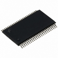
... Thin Shrink Small Outline Package (TSSOP), JEDEC MO-153, 6.1mm Wide (Note 3) Note 2: Ordering code “G” indicates Trays. Note 3: Devices also available in Tape and Reel. Specify by appending the suffix letter “X” to the ordering code. Logic Symbol © 2005 Fairchild Semiconductor Corporation Features 1.65V–3.6V V supply operation CC 3 ...
Page 2
Connection Diagrams Pin Assignment of TSSOP Pin Assignment for FBGA (Top Thru View) Logic Diagram www.fairchildsemi.com Pin Descriptions Pin Names Description OE Output Enable Input (Active LOW) n T/R Transmit/Receive Input n A –A Side A Inputs or 3-STATE Outputs ...
Page 3
Absolute Maximum Ratings Supply Voltage ( Input Voltage ( Output Voltage (V ) (Note 5) 0. Input Diode Current ( Output Diode Current ...
Page 4
AC Electrical Characteristics Symbol Parameter V 3.3V CC Min Propagation Delay 1.3 PHL PLH Output Enable Time 1.3 PZL PZH Output Disable Time 1.3 PLZ PHZ Capacitance Symbol Parameter C Input ...
Page 5
AC Loading and Waveforms FIGURE 1. AC Test Circuit (Input Characteristics: f Symbol r 3.3V 0. FIGURE 2. Waveform ...
Page 6
Physical Dimensions inches (millimeters) unless otherwise noted 54-Ball Fine-Pitch Ball Grid Array (FBGA), JEDEC MO-205, 5.5mm Wide www.fairchildsemi.com Package Number BGA54A 6 ...
Page 7
Physical Dimensions inches (millimeters) unless otherwise noted (Continued) 48-Lead Thin Shrink Small Outline Package (TSSOP), JEDEC MO-153, 6.1mm Wide Fairchild does not assume any responsibility for use of any circuitry described, no circuit patent licenses are implied and Fairchild reserves ...