NLU1GT125AMX1TCG ON Semiconductor, NLU1GT125AMX1TCG Datasheet - Page 3
NLU1GT125AMX1TCG
Manufacturer Part Number
NLU1GT125AMX1TCG
Description
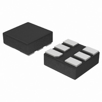
IC BUFF TRI-ST TTL N-INV 6ULLGA
Manufacturer
ON Semiconductor
Datasheet
1.NLU1GT125MUTCG.pdf
(8 pages)
Specifications of NLU1GT125AMX1TCG
Logic Type
Buffer/Line Driver, Non-Inverting
Number Of Elements
1
Number Of Bits Per Element
1
Current - Output High, Low
8mA, 8mA
Voltage - Supply
1.65 V ~ 5.5 V
Operating Temperature
-55°C ~ 125°C
Mounting Type
Surface Mount
Package / Case
6-ULLGA
Number Of Channels Per Chip
1
Polarity
Non-Inverting
Supply Voltage (max)
5.5 V
Supply Voltage (min)
1.65 V
Maximum Operating Temperature
+ 125 C
Mounting Style
Screw
High Level Output Current
- 8 mA
Low Level Output Current
8 mA
Minimum Operating Temperature
- 55 C
Number Of Lines (input / Output)
1 / 1
Output Type
3-State
Propagation Delay Time
11.5 ns at 3 V to 3.6 V, 7.5 ns at 4.5 V to 5.5 V
Lead Free Status / RoHS Status
Lead free / RoHS Compliant
Available stocks
Company
Part Number
Manufacturer
Quantity
Price
Company:

Part Number:
NLU1GT125AMX1TCG
Manufacturer:
ON Semiconductor
Quantity:
3 450


3. C
DC ELECTRICAL CHARACTERISTICS
AC ELECTRICAL CHARACTERISTICS
Symbol
Symbol
C
t
load. Average operating current can be obtained by the equation I
dynamic power consumption: P
I
t
t
V
I
t
t
t
C
V
PLH
V
I
OPD
I
PZL
PLZ
C
V
CCT
PHL
PZH
PHZ
I
OUT
CC
OZ
PD
OH
IN
OL
PD
IH
IN
IL
,
,
,
is defined as the value of the internal equivalent capacitance which is calculated from the dynamic operating current consumption without
Low-Level Input
Voltage
Low-Level Input
Voltage
High-Level Output
Voltage
Low-Level Output
Voltage
Input Leakage
Current
Quiescent Supply
Current
Quiescent Supply
Current
Output Leakage
Current
3-State Leakage
Current
Propagation Delay, A to Y
(Figures 3 and 5)
Output Enable Time, OE to Y
(Figures 4 and 6)
Output Disable Time, OE to Y
(Figures 4 and 6)
Input Capacitance
3-State Output Capacitance
(Output in High Impedance
State)
Power Dissipation
Capacitance (Note 3)
Parameter
Parameter
D
= C
V
I
V
I
I
V
I
V
I
I
0 v V
0 v V
V
Other Input: V
or GND
V
V
V
GND
PD
OH
OH
OH
OL
OL
OL
IN
IN
IN
IN
IN
OUT
IN
OUT
Conditions
• V
= 50 mA
= 4 mA
= 8 mA
= V
= -50 mA
= V
= -4 mA
= -8 mA
= V
= V
= 3.4 V
= V
= 5.5 V
= V
IN
IN
CC
IH
IH
IH
IH
IH
(Input t
3.0 to 3.6
4.5 to 5.5
3.0 to 3.6
4.5 to 5.5
3.0 to 3.6
4.5 to 5.5
v 5.5 V
v V
2
CC
or V
or V
or V
or V
or V
V
• f
(V)
5.0
CC
or
CC
in
IL
IL
IL
IL
CC
IL
r
+ I
= t
CC
http://onsemi.com
f
= 3.0 ns)
4.5 to 5.5
4.5 to 5.5
• V
NLU1GT125
V
0 to 5.5
C
C
C
C
C
C
C
C
C
C
C
C
Condition
CC
L
L
L
L
L
L
L
L
L
L
L
L
3.0
3.0
3.0
4.5
3.0
4.5
3.0
4.5
3.0
4.5
5.5
5.5
0.0
0.0
CC.
Test
= 15 pF
= 50 pF
= 15 pF
= 50 pF
= 15 pF
= 50 pF
= 15 pF
= 50 pF
= 15 pF
= 50 pF
= 15 pF
= 50 pF
(V)
3
CC(OPR)
2.58
3.94
Min
1.4
2.0
2.9
4.4
Min
= C
T
A
PD
T
Typ
= 25 5C
A
3.0
4.5
0
0
• V
= 25 5C
Typ
5.6
8.1
3.8
5.3
5.4
7.9
3.6
5.1
6.5
8.0
4.8
7.0
14
4
6
CC
±0.25
Max
0.53
0.36
0.36
±0.1
1.35
• f
0.8
0.1
0.1
1.0
0.5
Max
11.5
11.5
13.2
8.0
5.5
7.5
8.0
5.1
7.1
9.7
6.8
8.8
10
in
+ I
CC
2.48
3.80
Min
T
1.4
2.0
2.9
4.4
. C
Min
1.0
1.0
1.0
1.0
1.0
1.0
1.0
1.0
1.0
1.0
1.0
1.0
T
A
A
= +855C
PD
= +855C
is used to determine the no-load
Max
0.53
0.44
0.44
±1.0
1.50
±2.5
0.8
0.1
0.1
5.0
Max
13.0
13.0
11.5
15.0
10.0
20
9.5
6.5
8.5
9.5
6.0
8.0
8.0
10
2.34
3.66
Min
Min
T
1.4
2.0
2.9
4.4
T
to +1255C
to +1255C
A
A
= -555C
= -555C
Max
12.0
16.0
10.5
15.0
14.5
18.5
10.0
12.0
10.0
Max
0.53
0.52
0.52
±1.0
1.65
±2.5
11.5
0.8
0.1
0.1
8.5
7.5
9.5
40
10
Unit
Unit
mA
mA
mA
mA
mA
pF
pF
pF
ns
ns
ns
V
V
V
V
Related parts for NLU1GT125AMX1TCG
Image
Part Number
Description
Manufacturer
Datasheet
Request
R

Part Number:
Description:
Single Non Inverting Buffer, 3-state
Manufacturer:
ON Semiconductor
Datasheet:
Part Number:
Description:
ON Semiconductor [VOLTAGE REGULATOR]
Manufacturer:
ON Semiconductor
Datasheet:
Part Number:
Description:
357-036-542-201 CARDEDGE 36POS DL .156 BLK LOPRO
Manufacturer:
ON Semiconductor
Datasheet:
Part Number:
Description:
357-036-542-201 CARDEDGE 36POS DL .156 BLK LOPRO
Manufacturer:
ON Semiconductor
Datasheet:
Part Number:
Description:
357-036-542-201 CARDEDGE 36POS DL .156 BLK LOPRO
Manufacturer:
ON Semiconductor
Datasheet:
Part Number:
Description:
357-036-542-201 CARDEDGE 36POS DL .156 BLK LOPRO
Manufacturer:
ON Semiconductor
Datasheet:
Part Number:
Description:
357-036-542-201 CARDEDGE 36POS DL .156 BLK LOPRO
Manufacturer:
ON Semiconductor
Datasheet:
Part Number:
Description:
357-036-542-201 CARDEDGE 36POS DL .156 BLK LOPRO
Manufacturer:
ON Semiconductor
Datasheet:
Part Number:
Description:
357-036-542-201 CARDEDGE 36POS DL .156 BLK LOPRO
Manufacturer:
ON Semiconductor
Datasheet:
Part Number:
Description:
357-036-542-201 CARDEDGE 36POS DL .156 BLK LOPRO
Manufacturer:
ON Semiconductor
Datasheet:
Part Number:
Description:
357-036-542-201 CARDEDGE 36POS DL .156 BLK LOPRO
Manufacturer:
ON Semiconductor
Datasheet:
Part Number:
Description:
357-036-542-201 CARDEDGE 36POS DL .156 BLK LOPRO
Manufacturer:
ON Semiconductor
Datasheet:
Part Number:
Description:
Manufacturer:
ON Semiconductor
Datasheet:
Part Number:
Description:
Manufacturer:
ON Semiconductor
Datasheet: