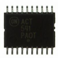
MC74ACT541DTG ON Semiconductor, MC74ACT541DTG Datasheet

MC74ACT541DTG
Specifications of MC74ACT541DTG
Related parts for MC74ACT541DTG
MC74ACT541DTG Summary of contents
Page 1
MC74AC540, MC74ACT540, MC74AC541, MC74ACT541 Octal Buffer/Line Driver with 3−State Outputs The MC74AC540/74ACT540 and MC74AC541/74ACT541 are octal buffer/line drivers designed to be employed as memory and address drivers, clock drivers and bus oriented transmitter/receivers. The MC74AC541/74ACT541 is a noninverting option of ...
Page 2
MC74AC540, MC74ACT540, MC74AC541, MC74ACT541 GND 10 Figure 1. MC74AC540/74ACT540 MAXIMUM RATINGS Symbol V DC Supply Voltage (Referenced to GND Input Voltage (Referenced to GND ...
Page 3
MC74AC540, MC74ACT540, MC74AC541, MC74ACT541 DC CHARACTERISTICS Symbol Parameter V Minimum High Level IH Input Voltage V Maximum Low Level IL Input Voltage V Minimum High Level OH Output Voltage V Maximum Low Level OL Output Voltage I Maximum Input IN ...
Page 4
MC74AC540, MC74ACT540, MC74AC541, MC74ACT541 AC CHARACTERISTICS (For Figures and Waveforms − See AND8277/D at www.onsemi.com) Symbol Parameter Propagation Delay t PLH ′ Data to Output ( AC540) Propagation Delay t PHL ′ Data to Output ( AC540) Output Enable Time ...
Page 5
MC74AC540, MC74ACT540, MC74AC541, MC74ACT541 DC CHARACTERISTICS Symbol Parameter V Minimum High Level IH Input Voltage V Maximum Low Level IL Input Voltage V Minimum High Level OH Output Voltage V Maximum Low Level OL Output Voltage I Maximum Input IN ...
Page 6
MC74AC540, MC74ACT540, MC74AC541, MC74ACT541 AC CHARACTERISTICS (For Figures and Waveforms − See AND8277/D at www.onsemi.com) Symbol Parameter Propagation Delay t PLH ′ Data to Output ( ACT540) Propagation Delay t PHL ′ Data to Output ( ACT540) Output Enable Time ...
Page 7
MC74AC540, MC74ACT540, MC74AC541, MC74ACT541 ORDERING INFORMATION Device MC74AC540N MC74AC540NG MC74ACT540N MC74ACT540NG MC74AC540DW MC74AC540DWG MC74AC540DWR2 MC74AC540DWR2G MC74ACT540DW MC74ACT540DWG MC74ACT540DWR2 MC74ACT540DWR2G MC74ACT540DTR2 MC74ACT540DTR2G MC74ACT540MEL MC74ACT540MELG MC74AC541N MC74AC541NG MC74ACT541N MC74ACT541NG MC74AC541DW MC74AC541DWG MC74AC541DWR2 MC74AC541DWR2G MC74ACT541DW MC74ACT541DWG MC74ACT541DWR2 MC74ACT541DWR2G †For information on tape and ...
Page 8
... MC74AC540, MC74ACT540, MC74AC541, MC74ACT541 ORDERING INFORMATION (continued) Device MC74AC541DTR2 MC74AC541DTR2G MC74ACT541DT MC74ACT541DTG MC74ACT541DTR2 MC74ACT541DTR2G MC74AC541M MC74AC541MG MC74AC541MEL MC74AC541MELG MC74ACT541M MC74ACT541MG MC74ACT541MEL MC74ACT541MELG †For information on tape and reel specifications, including part orientation and tape sizes, please refer to our Tape and Reel Packaging Specifications Brochure, BRD8011/D. *These packages are inherently Pb− ...
Page 9
MC74AC540, MC74ACT540, MC74AC541, MC74ACT541 PDIP− MC74AC54xN AWLYYWWG MC74ACT54xN AWLYYWWG 1 1 MARKING DIAGRAMS SOIC−20W TSSOP− AC54x 54x AWLYYWWG ALYWG ACT ACT54x 54x AWLYYWWG ALYWG ...
Page 10
MC74AC540, MC74ACT540, MC74AC541, MC74ACT541 −A− −T− SEATING PLANE 0.25 (0.010 20X 0. 18X A1 PACKAGE DIMENSIONS PDIP−20 ...
Page 11
... −V− 0.100 (0.004) −T− SEATING PLANE 16X 0.36 *For additional information on our Pb−Free strategy and soldering details, please download the ON Semiconductor Soldering and Mounting Techniques Reference Manual, SOLDERRM/D. PACKAGE DIMENSIONS TSSOP−20 DT SUFFIX CASE 948E−02 ISSUE Í ...
Page 12
... Opportunity/Affirmative Action Employer. This literature is subject to all applicable copyright laws and is not for resale in any manner. PUBLICATION ORDERING INFORMATION LITERATURE FULFILLMENT: Literature Distribution Center for ON Semiconductor P.O. Box 5163, Denver, Colorado 80217 USA Phone: 303−675−2175 or 800−344−3860 Toll Free USA/Canada Fax: 303− ...


