MC74VHC50D ON Semiconductor, MC74VHC50D Datasheet
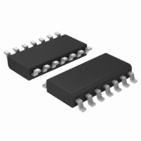
IC BUFFER HEX NON-INV 14SOIC

MC74VHC50D

Manufacturer Part Number
MC74VHC50D
Description
IC BUFFER HEX NON-INV 14SOIC
Manufacturer
ON Semiconductor
Series
74VHCr
Datasheet

Specifications of MC74VHC50D

Logic Type
Buffer/Line Driver, Non-Inverting
Number Of Elements
6
Number Of Bits Per Element
1
Current - Output High, Low
8mA, 8mA
Voltage - Supply
2 V ~ 5.5 V
Operating Temperature
-55°C ~ 125°C
Mounting Type
Surface Mount
Package / Case
14-SOIC (3.9mm Width), 14-SOL
Lead Free Status / RoHS Status
Contains lead / RoHS non-compliant

Available stocks

Company
Part Number
Manufacturer
Quantity
Price
Company:
Part Number:
MC74VHC50DR2G
Quantity:
301
Part Number:
MC74VHC50DTR2G
Manufacturer:
ON Semiconductor
Quantity:
3 950
MC74VHC50
Hex Buffer
fabricated with silicon gate CMOS technology.
output which provides high noise immunity and stable output. The
inputs tolerate voltages up to 7 V, allowing the interface of 5 V systems
to 3 V systems.
© Semiconductor Components Industries, LLC, 2006
March, 2006 - - Rev. 4
A1
A2
A3
A4
A5
A6
Figure 1. Logic Diagram
The MC74VHC50 is an advanced high speed CMOS buffer
The internal circuit is composed of three stages, including a buffered
These devices are available in Pb- -free package(s). Specifications herein
apply to both standard and Pb- -free devices. Please see our website at
www.onsemi.com for specific Pb- -free orderable part numbers, or
contact your local ON Semiconductor sales office or representative.
High Speed: t
Low Power Dissipation: I
High Noise Immunity: V
Power Down Protection Provided on Inputs
Balanced Propagation Delays
Designed for 2 V to 5.5 V Operating Range
Low Noise: V
1
3
5
9
11
13
PD
OLP
= 3.8 ns (Typ) at V
= 0.8 V (Max)
10
12
2
4
6
8
Y1
Y2
Y3
Y4
Y5
Y6
NIH
Y = A
CC
= 2 mA (Max) at T
= V
NIL
CC
= 28% V
A1
A2
A3
A4
A5
A6
= 5 V
Figure 2. Logic Symbol
CC
A
= 25°C
1
1
1
1
1
1
1
Y1
Y2
Y3
Y4
Y5
Y6
For detailed package marking information, see the Marking
Diagram section on page 4 of this data sheet.
MC74VHC50D
MC74VHC50M
14- -LEAD SOIC
V
Device
A1
14
CASE 751A
CC
1
MARKING DIAGRAM (Top View)
D SUFFIX
A Input
ORDERING INFORMATION
PIN CONNECTION AND
H
L
A6
Y1
13
2
FUNCTION TABLE
http://onsemi.com
http://onsemi.com
14- -LEAD SOIC EIAJ
Y6
A2
12
3
CASE 965
M SUFFIX
SOIC EIAJ
Package
SOIC
A5
Y2
11
Publication Order Number:
4
14- -LEAD TSSOP
Y5
A3
10
5
CASE 948G
DT SUFFIX
Y Output
MC74VHC50/D
55 Units/Rail
50 Units/Rail
A4
Y3
9
6
Shipping
H
L
GND
Y4
8
7

Related parts for MC74VHC50D

MC74VHC50D Summary of contents

Page 1

... For detailed package marking information, see the Marking Diagram section on page 4 of this data sheet MC74VHC50D MC74VHC50M Figure 2. Logic Symbol 1 http://onsemi.com http://onsemi.com 14- -LEAD SOIC 14- -LEAD TSSOP D SUFFIX DT SUFFIX CASE 751A CASE 948G 14- -LEAD SOIC EIAJ M SUFFIX CASE 965 PIN CONNECTION AND MARKING DIAGRAM (Top View ...

Page 2

MAXIMUM RATINGS Symbol V DC Supply Voltage Input Voltage Output Voltage OUT I DC Input Diode Current Output Diode Current Output Sink Current OUT I DC Supply Current ...

Page 3

DC ELECTRICAL CHARACTERISTICS Symbol Parameter V Minimum High--Level IH Input Voltage V Maximum Low--Level IL Input Voltage V V Minimum High--Level OH Output Voltage ...

Page 4

PLH PHL 50 Figure 3. Switching Waveforms INPUT Figure 5. Input Equivalent Circuit MARKING DIAGRAMS VHC50 AWLYWW 14- -LEAD SOIC D ...

Page 5

SEATING 14 PL PLANE 0.25 (0.010 PACKAGE DIMENSIONS SOIC- -14 D SUFFIX CASE 751A--03 ISSUE 0.25 (0.010) ...

Page 6

K 14X REF 0.10 (0.004) 0.15 (0.006 L PIN 1 IDENT. 1 0.15 (0.006 - 0.10 (0.004) - -T- - SEATING G D PLANE PACKAGE DIMENSIONS TSSOP ...

Page 7

... L DETAIL P VIEW American Technical Support: 800--282--9855 Toll Free USA/Canada Japan: ON Semiconductor, Japan Customer Focus Center 2--9--1 Kamimeguro, Meguro--ku, Tokyo, Japan 153--0051 Phone: 81--3--5773--3850 http://onsemi.com 7 NOTES: 1. DIMENSIONING AND TOLERANCING PER ANSI Y14.5M, 1982. 2. CONTROLLING DIMENSION: MILLIMETER. ...

Related keywords