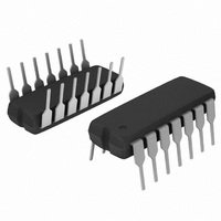
MC14024BCPG ON Semiconductor, MC14024BCPG Datasheet - Page 9

MC14024BCPG
Manufacturer Part Number
MC14024BCPG
Description
IC COUNTER RIPPLE 7STAGE 14DIP
Manufacturer
ON Semiconductor
Series
4000Br
Specifications of MC14024BCPG
Logic Type
Binary Counter
Direction
Up
Number Of Elements
1
Number Of Bits Per Element
7
Reset
Asynchronous
Count Rate
12MHz
Trigger Type
Positive, Negative
Voltage - Supply
3 V ~ 18 V
Operating Temperature
-55°C ~ 125°C
Mounting Type
Through Hole
Package / Case
14-DIP (0.300", 7.62mm)
Counter Type
Ripple
Counting Sequence
Up
Number Of Circuits
1
Logic Family
14024
Propagation Delay Time
2000 ns, 750 ns, 565 ns
Supply Voltage (max)
18 V
Maximum Operating Temperature
+ 125 C
Minimum Operating Temperature
- 55 C
Function
Counter/Divider
Mounting Style
Through Hole
Operating Supply Voltage
3 V to 18 V
Circuit Type
Low-Power Schottky
Current, Supply
600 μA
Function Type
7-Stages
Logic Function
Counter
Package Type
PDIP-14
Special Features
Ripple
Temperature, Operating, Range
-55 to +125 °C
Voltage, Supply
3 to 18 VDC
Lead Free Status / RoHS Status
Lead free / RoHS Compliant
Timing
-
Lead Free Status / Rohs Status
Lead free / RoHS Compliant
Other names
MC14024BCPGOS
PUBLICATION ORDERING INFORMATION
LITERATURE FULFILLMENT:
Literature Distribution Center for ON Semiconductor
P.O. Box 5163, Denver, Colorado 80217 USA
Phone: 303−675−2175 or 800−344−3860 Toll Free USA/Canada
Fax: 303−675−2176 or 800−344−3867 Toll Free USA/Canada
Email: orderlit@onsemi.com
ON Semiconductor and
to any products herein. SCILLC makes no warranty, representation or guarantee regarding the suitability of its products for any particular purpose, nor does SCILLC assume any liability
arising out of the application or use of any product or circuit, and specifically disclaims any and all liability, including without limitation special, consequential or incidental damages.
“Typical” parameters which may be provided in SCILLC data sheets and/or specifications can and do vary in different applications and actual performance may vary over time. All
operating parameters, including “Typicals” must be validated for each customer application by customer’s technical experts. SCILLC does not convey any license under its patent rights
nor the rights of others. SCILLC products are not designed, intended, or authorized for use as components in systems intended for surgical implant into the body, or other applications
intended to support or sustain life, or for any other application in which the failure of the SCILLC product could create a situation where personal injury or death may occur. Should
Buyer purchase or use SCILLC products for any such unintended or unauthorized application, Buyer shall indemnify and hold SCILLC and its officers, employees, subsidiaries, affiliates,
and distributors harmless against all claims, costs, damages, and expenses, and reasonable attorney fees arising out of, directly or indirectly, any claim of personal injury or death
associated with such unintended or unauthorized use, even if such claim alleges that SCILLC was negligent regarding the design or manufacture of the part. SCILLC is an Equal
Opportunity/Affirmative Action Employer. This literature is subject to all applicable copyright laws and is not for resale in any manner.
e
0.13 (0.005)
14
1
Z
b
M
D
are registered trademarks of Semiconductor Components Industries, LLC (SCILLC). SCILLC reserves the right to make changes without further notice
8
7
0.10 (0.004)
A
E
A
H
1
E
VIEW P
N. American Technical Support: 800−282−9855 Toll Free
Europe, Middle East and Africa Technical Support:
Japan Customer Focus Center
PACKAGE DIMENSIONS
M
USA/Canada
Phone: 421 33 790 2910
Phone: 81−3−5773−3850
_
L
E
http://onsemi.com
CASE 965−01
SOEIAJ−14
L
DETAIL P
ISSUE A
9
Q
1
c
NOTES:
1. DIMENSIONING AND TOLERANCING PER ANSI
2. CONTROLLING DIMENSION: MILLIMETER.
3. DIMENSIONS D AND E DO NOT INCLUDE MOLD
4. TERMINAL NUMBERS ARE SHOWN FOR
5. THE LEAD WIDTH DIMENSION (b) DOES NOT
ON Semiconductor Website: www.onsemi.com
Order Literature: http://www.onsemi.com/orderlit
For additional information, please contact your local
Sales Representative
Y14.5M, 1982.
FLASH OR PROTRUSIONS AND ARE MEASURED
AT THE PARTING LINE. MOLD FLASH OR
PROTRUSIONS SHALL NOT EXCEED 0.15 (0.006)
PER SIDE.
REFERENCE ONLY.
INCLUDE DAMBAR PROTRUSION. ALLOWABLE
DAMBAR PROTRUSION SHALL BE 0.08 (0.003)
TOTAL IN EXCESS OF THE LEAD WIDTH
DIMENSION AT MAXIMUM MATERIAL CONDITION.
DAMBAR CANNOT BE LOCATED ON THE LOWER
RADIUS OR THE FOOT. MINIMUM SPACE
BETWEEN PROTRUSIONS AND ADJACENT LEAD
TO BE 0.46 ( 0.018).
H
0.50
DIM
A
L
Q
M
A
b
D
E
Z
c
e
E
1
E
1
MILLIMETERS
MIN
0.05
0.35
0.10
9.90
5.10
7.40
0.50
0.70
1.10
−−−
−−−
0
1.27 BSC
_
10.50
MAX
10
2.05
0.20
0.50
0.20
5.45
8.20
0.85
1.50
0.90
1.42
_
0.002
0.014
0.004
0.390
0.201
0.291
0.020
0.043
0.028
MIN
−−−
−−−
0.050 BSC
0
INCHES
_
MC14024B/D
0.081
0.008
0.020
0.008
0.413
0.215
0.323
0.033
0.059
0.035
0.056
MAX
10
_


