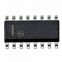
MC14060BDG ON Semiconductor, MC14060BDG Datasheet - Page 2

MC14060BDG
Manufacturer Part Number
MC14060BDG
Description
IC COUNTER/OSC 14BIT BIN 16-SOIC
Manufacturer
ON Semiconductor
Series
4000Br
Type
Binaryr
Specifications of MC14060BDG
Logic Type
Binary Counter
Direction
Up
Number Of Elements
1
Number Of Bits Per Element
14
Count Rate
17MHz
Trigger Type
Negative Edge
Voltage - Supply
3 V ~ 18 V
Operating Temperature
-55°C ~ 125°C
Mounting Type
Surface Mount
Package / Case
16-SOIC (3.9mm Width)
Counter Type
Binary
Counting Sequence
Up
Number Of Circuits
1
Logic Family
14060
Propagation Delay Time
740 ns, 300 ns, 200 ns
Supply Voltage (max)
18 V
Maximum Operating Temperature
+ 125 C
Minimum Operating Temperature
- 55 C
Function
Counter/Divider
Mounting Style
SMD/SMT
Operating Supply Voltage
3 V to 18 V
Circuit Type
Low-Power Schottky
Current, Supply
600 μA
Function Type
14-Bits
Logic Function
Counter/Oscillator
Package Type
SOIC-16
Special Features
Binary
Temperature, Operating, Range
-55 to +125 °C
Voltage, Supply
3 to 18 VDC
Technology
CMOS
Number Of Elements
1
Number Of Bits
14
Logical Function
Counter/Divider
Operating Supply Voltage (typ)
3.3/5/9/12/15V
Operating Temp Range
-55C to 125C
Operating Supply Voltage (min)
3V
Operating Supply Voltage (max)
18V
Operating Temperature Classification
Military
Mounting
Surface Mount
Pin Count
16
Lead Free Status / RoHS Status
Lead free / RoHS Compliant
Reset
-
Timing
-
Lead Free Status / Rohs Status
Lead free / RoHS Compliant
Other names
MC14060BDG
MC14060BDGOS
MC14060BDGOS
†For information on tape and reel specifications, including part orientation and tape sizes, please refer to our Tape and Reel Packaging
*This package is inherently Pb−Free.
ORDERING INFORMATION
Specifications Brochure, BRD8011/D.
10
12
MC14060BCP
MC14060BCPG
MC14060BD
MC14060BDG
MC14060BDR2
MC14060BDR2G
MC14060BDTR2
MC14060BFEL
11
9
OUT 2
OUT 1
CLOCK
RESET
Figure 1. Pin Assignment
Device
Q12
Q13
Q14
V
Q6
Q5
Q7
Q4
SS
1
2
3
4
5
6
7
8
16
15
14
13
12
10
11
9
V
Q10
Q8
Q9
RESET
CLOCK
OUT 1
OUT 2
DD
Figure 2. Logic Diagram
http://onsemi.com
TSSOP−16*
SOEIAJ−16
C
C
(Pb−Free)
(Pb−Free)
(Pb−Free)
(Pb−Free)
Package
PDIP−16
PDIP−16
SOIC−16
SOIC−16
SOIC−16
SOIC−16
MC14060B
R
Q
Q
2
C
C
Table 1. Truth Table
X = Don’t Care
R
Q
Q
Clock
H
Q4
7
Q6 = PIN 4
Q7 = PIN 6
C
C
R
Q
Q
Reset
Q5
H
Q8 = PIN 14
Q9 = PIN 13
L
L
5
C
C
R
Q
Q
2500 / Tape & Reel
2500 / Tape & Reel
2500 / Tape & Reel
2000 / Tape & Reel
No Change
Advance to Next State
All Outputs are Low
500 Units / Rail
500 Units / Rail
48 Units / Rail
48 Units / Rail
Q12
Shipping
Q10 = PIN 15
1
C
C
R
Output State
Q
Q
†
Q13
2
V
V
C
C
DD
SS
R
= PIN 8
= PIN 16
Q
Q
Q14
3


