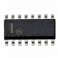
MC74HC4060ADG ON Semiconductor, MC74HC4060ADG Datasheet - Page 6

MC74HC4060ADG
Manufacturer Part Number
MC74HC4060ADG
Description
IC COUNTER 14STAGE BIN 16-SOIC
Manufacturer
ON Semiconductor
Series
74HCr
Datasheet
1.MC74HC4060ADR2.pdf
(14 pages)
Specifications of MC74HC4060ADG
Logic Type
Binary Counter
Direction
Up
Number Of Elements
1
Number Of Bits Per Element
14
Reset
Asynchronous
Count Rate
50MHz
Trigger Type
Negative Edge
Voltage - Supply
2 V ~ 6 V
Operating Temperature
-55°C ~ 125°C
Mounting Type
Surface Mount
Package / Case
16-SOIC (3.9mm Width)
Lead Free Status / RoHS Status
Lead free / RoHS Compliant
Timing
-
Other names
MC74HC4060ADG
MC74HC4060ADGOS
MC74HC4060ADGOS
INPUTS
Osc In (Pin 11)
transition on this input advances the state of the counter. Osc
In may be driven by an external clock source.
Reset (Pin 12)
asynchronously resets the counter to its zero state (forcing
all Q outputs low) and disables the oscillator.
OUTPUTS
Q4—Q10, Q12−Q14 (Pins 7, 5, 4, 6, 13, 15, 1, 2, 3)
input frequency by 2
and Q11 are not available as outputs.
Negative−edge triggering clock input. A high−to−low
Active−high reset. A high level applied to this input
Active−high outputs. Each Qn output divides the Clock
Osc In
Qn+1
Q
Qn
10%
50%
90%
90%
50%
10%
50%
t
PLH
N
t
f
t
. The user should note the Q1, Q2, Q3
t
PLH
w
t
TLH
50%
Figure 1.
Figure 3.
1/f
MAX
t
r
t
PHL
t
PHL
t
THL
SWITCHING WAVEFORMS
PIN DESCRIPTIONS
http://onsemi.com
MC74HC4060A
V
GND
CC
V
GND
CC
6
Osc Out 1, Osc Out 2 (Pins 9, 10)
with Osc In and the external components to form an
oscillator. When Osc In is being driven with an external
clock source, Osc Out 1 and Osc Out 2 must be left open
circuited. With the crystal oscillator configuration in Figure
6, Osc Out 2 must be left open circuited.
Oscillator outputs. These pins are used in conjunction
Osc In
Reset
Q
*Includes all probe and jig capacitance
t
PHL
Figure 4. Test Circuit
DEVICE
UNDER
TEST
Figure 2.
50%
50%
OUTPUT
t
w
POINT
TEST
t
rec
50%
C
L
*
V
GND
V
GND
CC
CC


