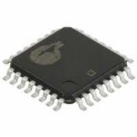
CY7C4211-10AXI Cypress Semiconductor Corp, CY7C4211-10AXI Datasheet - Page 8

CY7C4211-10AXI
Manufacturer Part Number
CY7C4211-10AXI
Description
IC SYNC FIFO MEM 512X9 32-TQFP
Manufacturer
Cypress Semiconductor Corp
Series
CY7Cr
Specifications of CY7C4211-10AXI
Function
Synchronous
Memory Size
4.6K (512 x 9)
Data Rate
100MHz
Access Time
8ns
Voltage - Supply
3.3V
Operating Temperature
-40°C ~ 85°C
Mounting Type
Surface Mount
Package / Case
32-TQFP
Configuration
Dual
Density
4Kb
Access Time (max)
8ns
Word Size
9b
Organization
512x9
Sync/async
Synchronous
Expandable
Yes
Bus Direction
Uni-Directional
Clock Freq (max)
100MHz
Operating Supply Voltage (typ)
5V
Operating Supply Voltage (min)
4.5V
Operating Supply Voltage (max)
5.5V
Supply Current
40mA
Operating Temp Range
-40C to 85C
Operating Temperature Classification
Industrial
Mounting
Surface Mount
Pin Count
32
Lead Free Status / RoHS Status
Lead free / RoHS Compliant
Available stocks
Company
Part Number
Manufacturer
Quantity
Price
Company:
Part Number:
CY7C4211-10AXI
Manufacturer:
Cypress Semiconductor Corp
Quantity:
10 000
Company:
Part Number:
CY7C4211-10AXIT
Manufacturer:
Cypress Semiconductor Corp
Quantity:
10 000
Document #: 38-06016 Rev. *C
AC Test Loads and Waveforms
Switching Characteristics
t
t
t
t
t
t
t
t
t
t
t
t
t
t
t
t
t
t
t
t
t
t
Notes:
11. C
12. C
13. Pulse widths less than minimum values are not allowed.
14. Values guaranteed by design, not currently tested.
S
A
CLK
CLKH
CLKL
DS
DH
ENS
ENH
RS
RSS
RSR
RSF
OLZ
OE
OHZ
WFF
REF
PAF
PAE
SKEW1
SKEW2
Parameter
L
L
= 30 pF for all AC parameters except for t
= 5 pF for t
Clock Cycle Frequency
Data Access Time
Clock Cycle Time
Clock HIGH Time
Clock LOW Time
Data Set-up Time
Data Hold Time
Enable Set-up Time
Enable Hold Time
Reset Pulse Width
Reset Set-up Time
Reset Recovery Time
Reset to Flag and Output Time
Output Enable to Output in Low-Z
Output Enable to Output Valid
Output Enable to Output in High-Z
Write Clock to Full Flag
Read Clock to Empty Flag
Clock to Programmable Almost-Full Flag
Clock to Programmable Almost-Full Flag
Skew Time between Read Clock and Write Clock
for Empty Flag and Full Flag
Skew Time between Read Clock and Write Clock
for Almost-Empty Flag and Almost-Full Flag
OHZ
OUTPUT
.
INCLUDING
5V
JIG AND
SCOPE
C
L
Description
[13]
R1 1.1 K Ω
Over the Operating Range
OHZ
Equivalent to:
[11, 12]
.
R2
680Ω
[14]
[14]
OUTPUT
THÉ VENIN EQUIVALENT
Min.
4.5
4.5
0.5
0.5
10
10
10
2
3
3
8
8
0
3
3
5
GND
3.0V
420Ω
-10
≤ 3 ns
Max.
100
10
8
7
7
8
8
8
8
CY7C4421/4201/4211/4221
1.91V
Min.
15
15
10
10
15
ALL INPUT PULSES
2
6
6
4
1
4
1
0
3
3
6
10%
90%
-15
CY7C4231/4241/4251
Max.
66.7
10
15
10
10
10
10
8
8
Min.
25
10
10
25
15
15
10
18
2
6
1
6
1
0
3
3
90%
-25
10%
Max.
≤ 3 ns
40
15
25
12
12
15
15
15
15
Page 8 of 19
MHz
Unit
ns
ns
ns
ns
ns
ns
ns
ns
ns
ns
ns
ns
ns
ns
ns
ns
ns
ns
ns
ns
ns
[+] Feedback


