74HC574DTR2G ON Semiconductor, 74HC574DTR2G Datasheet - Page 3
74HC574DTR2G
Manufacturer Part Number
74HC574DTR2G
Description
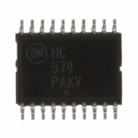
IC FLIP FLOP OCT 3ST D 20-TSSOP
Manufacturer
ON Semiconductor
Series
74HCr
Type
D-Type Busr
Datasheet
1.74HC574DTR2G.pdf
(8 pages)
Specifications of 74HC574DTR2G
Function
Standard
Output Type
Tri-State Non Inverted
Number Of Elements
1
Number Of Bits Per Element
8
Frequency - Clock
28MHz
Delay Time - Propagation
34ns
Trigger Type
Positive Edge
Current - Output High, Low
7.8mA, 7.8mA
Voltage - Supply
2 V ~ 6 V
Operating Temperature
-55°C ~ 125°C
Mounting Type
Surface Mount
Package / Case
20-TSSOP
Lead Free Status / RoHS Status
Lead free / RoHS Compliant
Other names
74HC574DTR2GOSTR


Stresses exceeding Maximum Ratings may damage the device. Maximum Ratings are stress ratings only. Functional operation above the
Recommended Operating Conditions is not implied. Extended exposure to stresses above the Recommended Operating Conditions may affect
device reliability.
1. I
2. Tested to EIA/JESD22−A114−A.
3. Tested to EIA/JESD22−A115−A.
4. Tested to EIA/JESD78.
5. For high frequency or heavy load considerations, see the ON Semiconductor High−Speed CMOS Data Book (DL129/D).
6. Unused inputs may not be left open. All inputs must be tied to a high− or low−logic input voltage level.
†For information on tape and reel specifications, including part orientation and tape sizes, please refer to our Tape and Reel Packaging
*This package is inherently Pb−Free.
RECOMMENDED OPERATING CONDITIONS
MAXIMUM RATINGS
ORDERING INFORMATION
Specifications Brochure, BRD8011/D.
74HC574DTR2G
Symbol
Symbol
I
V
Latchup
V
T
I
MSL
V
V
O
I
I
GND
q
t
V
I
P
F
I
STG
T
T
ESD
T
r
V
OK
I
CC
, V
, t
CC
IK
CC
O
JA
R
A
O
L
D
J
absolute maximum rating must be observed.
I
f
O
DC Supply Voltage
DC Input Voltage
DC Output Voltage
DC Input Diode Current
DC Output Diode Current
DC Output Sink Current
DC Supply Current per Supply Pin
DC Ground Current per Ground Pin
Storage Temperature Range
Lead Temperature, 1 mm from Case for 10 Seconds
Junction Temperature under Bias
Thermal Resistance
Power Dissipation in Still Air at 85_C
Moisture Sensitivity
Flammability Rating
ESD Withstand Voltage
Latchup Performance
DC Supply Voltage
DC Input Voltage, Output Voltage
Operating Temperature, All Package Types
Input Rise and Fall Time (Figure 3)
Device
Parameter
Parameter
Above V
http://onsemi.com
CC
and Below GND at 85_C (Note 4)
TSSOP−20*
Package
Human Body Model (Note 2)
3
Oxygen Index: 30% − 35%
Machine Model (Note 3)
(Referenced to GND)
(Referenced to GND)
V
V
V
CC
CC
CC
(Note 1)
TSSOP
TSSOP
= 2.0 V
= 4.5 V
= 6.0 V
UL 94 V−0 @ 0.125 in
*55
Min
*0.5 to V
*0.5 to V
2.0
0
0
0
0
2500 / Tape & Reel
*0.5 to )7.0
*65 to )150
Level 1
Shipping
>2000
Value
)150
$300
>200
$20
$35
$35
$75
$75
260
128
450
CC
CC
)0.5
)0.5
)125
1000
Max
V
500
400
6.0
†
CC
_C/W
Unit
Unit
mW
mA
mA
mA
mA
mA
mA
_C
_C
_C
_C
ns
V
V
V
V
V
V
Related parts for 74HC574DTR2G
Image
Part Number
Description
Manufacturer
Datasheet
Request
R

Part Number:
Description:
ON Semiconductor [VOLTAGE REGULATOR]
Manufacturer:
ON Semiconductor
Datasheet:
Part Number:
Description:
357-036-542-201 CARDEDGE 36POS DL .156 BLK LOPRO
Manufacturer:
ON Semiconductor
Datasheet:
Part Number:
Description:
357-036-542-201 CARDEDGE 36POS DL .156 BLK LOPRO
Manufacturer:
ON Semiconductor
Datasheet:
Part Number:
Description:
357-036-542-201 CARDEDGE 36POS DL .156 BLK LOPRO
Manufacturer:
ON Semiconductor
Datasheet:
Part Number:
Description:
357-036-542-201 CARDEDGE 36POS DL .156 BLK LOPRO
Manufacturer:
ON Semiconductor
Datasheet:
Part Number:
Description:
357-036-542-201 CARDEDGE 36POS DL .156 BLK LOPRO
Manufacturer:
ON Semiconductor
Datasheet:
Part Number:
Description:
357-036-542-201 CARDEDGE 36POS DL .156 BLK LOPRO
Manufacturer:
ON Semiconductor
Datasheet:
Part Number:
Description:
357-036-542-201 CARDEDGE 36POS DL .156 BLK LOPRO
Manufacturer:
ON Semiconductor
Datasheet:
Part Number:
Description:
357-036-542-201 CARDEDGE 36POS DL .156 BLK LOPRO
Manufacturer:
ON Semiconductor
Datasheet:
Part Number:
Description:
357-036-542-201 CARDEDGE 36POS DL .156 BLK LOPRO
Manufacturer:
ON Semiconductor
Datasheet:
Part Number:
Description:
357-036-542-201 CARDEDGE 36POS DL .156 BLK LOPRO
Manufacturer:
ON Semiconductor
Datasheet:
Part Number:
Description:
Manufacturer:
ON Semiconductor
Datasheet:
Part Number:
Description:
Manufacturer:
ON Semiconductor
Datasheet:
Part Number:
Description:
Manufacturer:
ON Semiconductor
Datasheet: