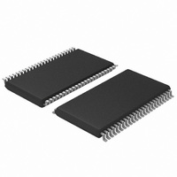
MC74LCX16374DTG ON Semiconductor, MC74LCX16374DTG Datasheet - Page 4

MC74LCX16374DTG
Manufacturer Part Number
MC74LCX16374DTG
Description
IC FLIP FLOP 16BIT D LV 48-TSSOP
Manufacturer
ON Semiconductor
Series
74LCXr
Type
D-Type Busr
Datasheet
1.MC74LCX16374DTG.pdf
(7 pages)
Specifications of MC74LCX16374DTG
Function
Standard
Output Type
Tri-State Non Inverted
Number Of Elements
2
Number Of Bits Per Element
8
Frequency - Clock
170MHz
Delay Time - Propagation
1.5ns
Trigger Type
Positive Edge
Current - Output High, Low
24mA, 24mA
Voltage - Supply
2 V ~ 3.6 V
Operating Temperature
-40°C ~ 85°C
Mounting Type
Surface Mount
Package / Case
48-TSSOP
Number Of Circuits
16
Logic Family
74LC
Logic Type
D-Type Flip-Flop
Polarity
Non-Inverting
Input Type
Single-Ended
Propagation Delay Time
6.5 ns
High Level Output Current
- 24 mA
Supply Voltage (max)
3.6 V
Maximum Operating Temperature
+ 85 C
Mounting Style
SMD/SMT
Minimum Operating Temperature
- 40 C
Supply Voltage (min)
2 V
Lead Free Status / RoHS Status
Lead free / RoHS Compliant
Other names
MC74LCX16374DTG
MC74LCX16374DTGOS
MC74LCX16374DTGOS
Available stocks
Company
Part Number
Manufacturer
Quantity
Price
Company:
Part Number:
MC74LCX16374DTG
Manufacturer:
ON Semiconductor
Quantity:
13
2. These values of V
3. Skew is defined as the absolute value of the difference between the actual propagation delay for any two separate outputs of the same device.
DC ELECTRICAL CHARACTERISTICS
AC CHARACTERISTICS
Symbol
Symbol
t
t
DI
V
I
t
t
t
t
OSHL
OSLH
V
f
t
t
The specification applies to any outputs switching in the same direction, either HIGH−to−LOW (t
guaranteed by design.
V
I
V
I
OFF
max
PLH
PHL
PZH
PHZ
PZL
PLZ
OZ
CC
t
t
t
OH
OL
I
w
IH
CC
s
h
IL
I
HIGH Level Input Voltage (Note 2)
LOW Level Input Voltage (Note 2)
HIGH Level Output Voltage
LOW Level Output Voltage
Input Leakage Current
3−State Output Current
Power−Off Leakage Current
Quiescent Supply Current
Increase in I
Clock Pulse Frequency
Propagation Delay
CP to O
Output Enable Time to
High and Low Level
Output Disable Time From
High and Low Level
Setup Time, HIGH or LOW D
CP
Hold Time, HIGH or LOW D
CP Pulse Width, HIGH
Output−to−Output Skew
(Note 3)
n
I
are used to test DC electrical characteristics only.
Parameter
CC
Characteristic
per Input
t
R
= t
F
= 2.5 ns; C
n
n
to CP
to
L
Waveform
= 50 pF; R
1
1
2
2
1
1
3
http://onsemi.com
2.3 ≤ V
L
= 500 W
2.3 V ≤ V
2.3 ≤ V
2.3 ≤ V
2.3 ≤ V
V
2.3 V ≤ V
2.3 V ≤ V
CC
Min
170
1.5
1.5
1.5
1.5
1.5
1.5
2.5
1.5
3.0
V
V
V
V
CC
C
V
V
V
= 3.3 V ± 0.3 V
V
CC
CC
CC
CC
4
V
L
CC
CC
CC
CC
CC
CC
CC
CC
2.3 V ≤ V
2.7 V ≤ V
2.3 V ≤ V
2.7 V ≤ V
≤ 3.6 V; 3.6 ≤ V
= 50 pF
CC
= 0 V; V
= 2.7 V; I
= 3.0 V; I
= 3.0 V; I
= 2.3 V; I
= 3.0 V; I
= 3.0 V; I
≤ 3.6 V; V
CC
CC
= 2.7 V; I
≤ 3.6 V; V
V
≤ 3.6 V; 0V ≤ V
= 2.3 V; I
I
≤ 3.6 V; 0 V ≤ V
Condition
= V
≤ 3.6 V; I
≤ 3.6 V; I
Max
6.2
6.2
6.1
6.1
6.0
6.0
1.0
1.0
IH
I
CC
CC
CC
CC
OH
OH
OH
or V
OH
OL
OL
or V
OL
IH
OL
I
≤ 2.7 V
≤ 3.6 V
≤ 2.7 V
≤ 3.6 V
= GND or V
= −12 mA
= −18 mA
= −24 mA
= 12 mA
= 16 mA
= 24 mA
= −8 mA
O
= V
T
= 8 mA
OL
OL
I
A
IL
= 5.5 V
or V
= −55°C to +125°C
= 100 mA
= 100 mA
O
CC
Min
1.5
1.5
1.5
1.5
1.5
1.5
2.5
1.5
3.0
V
I
≤ 5.5 V;
C
O
≤ 5.5 V
− 0.6 V
CC
L
≤ 5.5 V
= 50 pF
= 2.7 V
CC
OSHL
Max
6.5
6.5
6.3
6.3
6.2
6.2
) or LOW−to−HIGH (t
V
T
CC
A
Min
1.7
2.0
1.8
2.2
2.4
2.2
V
= −55°C to +125°C
− 0.2
CC
Min
1.5
1.5
1.5
1.5
1.5
1.5
3.0
2.0
3.5
C
= 2.5 V ± 0.2 V
L
= 30 pF
Max
0.55
±5.0
±5.0
OSLH
±20
500
0.7
0.8
0.2
0.6
0.4
0.4
Max
10
20
7.4
7.4
7.9
7.9
7.2
7.2
); parameter
MHz
Unit
Unit
mA
mA
mA
mA
mA
mA
ns
ns
ns
ns
ns
ns
ns
V
V
V
V


