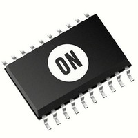
MC74AC574DTR2G ON Semiconductor, MC74AC574DTR2G Datasheet

MC74AC574DTR2G
Specifications of MC74AC574DTR2G
MC74AC574DTR2GOSTR
Related parts for MC74AC574DTR2G
MC74AC574DTR2G Summary of contents
Page 1
MC74AC574, MC74ACT574 Octal D Flip−Flop with 3−State Outputs The MC74AC574/74ACT574 is a high−speed, low power octal flip−flop with a buffered common Clock (CP) and a buffered common Output Enable (OE). The information presented to the D inputs is stored in ...
Page 2
FUNCTIONAL DESCRIPTION The MC74AC574/74ACT574 consists of eight edge- triggered flip−flops with individual D−type inputs and 3−state true outputs. The buffered clock and buffered Output Enable are common to all flip−flops. The eight flip−flops will store the state of their individual ...
Page 3
RECOMMENDED OPERATING CONDITIONS Symbol V Supply Voltage Input Voltage, Output Voltage (Ref. to GND) IN OUT Input Rise and Fall Time (Note ′AC Devices except Schmitt Inputs Input Rise ...
Page 4
AC CHARACTERISTICS (For Figures and Waveforms − See AND8277/D at www.onsemi.com) Symbol Parameter Maximum Clock f max Frequency Propagation Delay t PLH Propagation Delay t PHL Output Enable Time PZH t ...
Page 5
DC CHARACTERISTICS Symbol Parameter V Minimum High Level IH Input Voltage V Maximum Low Level IL Input Voltage V Minimum High Level OH Output Voltage V Maximum Low Level OL Output Voltage I Maximum Input IN Leakage Current DI Additional ...
Page 6
AC OPERATING REQUIREMENTS Symbol Parameter Setup Time, HIGH or LOW Hold Time, HIGH or LOW Pulse Width t w HIGH or LOW *Voltage Range 3 ...
Page 7
... MC74ACT574N MC74ACT574NG MC74AC574DW MC74AC574DWG MC74AC574DWR2 MC74AC574DWR2G MC74ACT574DW MC74ACT574DWG MC74ACT574DWR2 MC74ACT574DWR2G MC74AC574DTR2 MC74AC574DTR2G MC74ACT574DTR2 MC74ACT574DTR2G MC74AC574M MC74AC574MG MC74AC574MEL MC74AC574MELG MC74ACT574M MC74ACT574MG MC74ACT574MEL MC74ACT574MELG †For information on tape and reel specifications, including part orientation and tape sizes, please refer to our Tape and Reel Packaging Specifications Brochure, BRD8011/D. *These packages are inherently Pb− ...
Page 8
SEATING PLANE 0.25 (0.010 20X 0. 18X A1 MC74AC574, MC74ACT574 PACKAGE DIMENSIONS PDIP−20 N SUFFIX ...
Page 9
... 0.100 (0.004) −T− SEATING PLANE 16X 0.36 *For additional information on our Pb−Free strategy and soldering details, please download the ON Semiconductor Soldering and Mounting Techniques Reference Manual, SOLDERRM/D. MC74AC574, MC74ACT574 PACKAGE DIMENSIONS TSSOP−20 DT SUFFIX CASE 948E−02 ISSUE ...
Page 10
... Opportunity/Affirmative Action Employer. This literature is subject to all applicable copyright laws and is not for resale in any manner. PUBLICATION ORDERING INFORMATION LITERATURE FULFILLMENT: Literature Distribution Center for ON Semiconductor P.O. Box 5163, Denver, Colorado 80217 USA Phone: 303−675−2175 or 800−344−3860 Toll Free USA/Canada Fax: 303− ...


