MC74ACT574NG ON Semiconductor, MC74ACT574NG Datasheet - Page 3
MC74ACT574NG
Manufacturer Part Number
MC74ACT574NG
Description
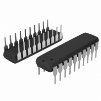
IC FLIP-FLOP OCT 20-DIP
Manufacturer
ON Semiconductor
Series
74ACTr
Type
D-Type Busr
Datasheet
1.MC74AC574DWG.pdf
(10 pages)
Specifications of MC74ACT574NG
Function
Standard
Output Type
Tri-State Non Inverted
Number Of Elements
1
Number Of Bits Per Element
8
Frequency - Clock
100MHz
Delay Time - Propagation
2.5ns
Trigger Type
Positive Edge
Current - Output High, Low
24mA, 24mA
Voltage - Supply
4.5 V ~ 5.5 V
Operating Temperature
-40°C ~ 85°C
Mounting Type
Through Hole
Package / Case
20-DIP (0.300", 7.62mm)
Logic Family
ACT
Technology
CMOS
Number Of Bits
8
Number Of Elements
1
Clock-edge Trigger Type
Positive-Edge
Polarity
Non-Inverting
Operating Supply Voltage (typ)
5V
Package Type
PDIP
Propagation Delay Time
12ns
Low Level Output Current
24mA
High Level Output Current
-24mA
Operating Supply Voltage (min)
4.5V
Operating Supply Voltage (max)
5.5V
Operating Temp Range
-40C to 85C
Operating Temperature Classification
Industrial
Mounting
Through Hole
Pin Count
20
Lead Free Status / RoHS Status
Lead free / RoHS Compliant


1. V
2. V
* All outputs loaded; thresholds on input associated with output under test.
†Maximum test duration 2.0 ms, one output loaded at a time.
NOTE:
RECOMMENDED OPERATING CONDITIONS
DC CHARACTERISTICS
V
Symbol
Symbol
IN
I
I
V
V
IN
IN
V
OHD
V
V
OLD
I
, V
t
t
I
I
I
CC
T
T
OH
r
r
OH
OL
IN
OL
, t
, t
IH
CC
IL
A
from 30% to 70% V
from 0.8 V to 2.0 V; see individual Data Sheets for devices that differ from the typical input rise and fall times.
J
OUT
f
f
Note: I
Minimum High Level
Input Voltage
Maximum Low Level
Input Voltage
Minimum High Level
Output Voltage
Maximum Low Level
Output Voltage
Maximum Input
Leakage Current
†Minimum Dynamic
Maximum Quiescent Supply Current
Output Current
Supply Voltage
DC Input Voltage, Output Voltage (Ref. to GND)
Input Rise and Fall Time (Note 1)
′AC Devices except Schmitt Inputs
Input Rise and Fall Time (Note 2)
′ACT Devices except Schmitt Inputs
Junction Temperature (PDIP)
Operating Ambient Temperature Range
Output Current − High
Output Current − Low
IN
and I
CC
CC
@ 3.0 V are guaranteed to be less than or equal to the respective limit @ 5.5 V V
; see individual Data Sheets for devices that differ from the typical input rise and fall times.
Parameter
Parameter
MC74AC574, MC74ACT574
http://onsemi.com
V
(V)
3.0
4.5
5.5
3.0
4.5
5.5
3.0
4.5
5.5
3.0
4.5
5.5
3.0
4.5
5.5
3.0
4.5
5.5
5.5
5.5
5.5
5.5
CC
0.002
0.001
0.001
2.25
2.75
2.25
2.75
2.99
4.49
5.49
Typ
T
1.5
1.5
3
−
−
−
−
−
−
−
−
−
−
A
74AC
= +25°C
V
V
V
V
V
CC
CC
CC
CC
CC
′ACT
3.15
3.85
1.35
1.65
2.56
3.86
4.86
0.36
0.36
0.36
±0.1
′AC
@ 3.0 V
@ 4.5 V
@ 5.5 V
@ 4.5 V
@ 5.5 V
2.1
0.9
2.9
4.4
5.4
0.1
0.1
0.1
8.0
−
−
Guaranteed Limits
T
A
= −40°C to +85°C
Min
−40
74AC
2.0
4.5
3.15
3.85
1.35
1.65
2.46
3.76
4.76
0.44
0.44
0.44
±1.0
−75
2.1
0.9
2.9
4.4
5.4
0.1
0.1
0.1
0
−
−
−
−
−
−
−
−
75
80
Typ
150
5.0
5.0
8.0
40
25
10
25
−
−
−
−
Unit
CC
mA
mA
mA
mA
V
V
V
V
V
V
.
Max
V
or V
V
or V
I
*V
I
I
*V
I
V
V
V
V
V
140
−24
6.0
5.5
OUT
OH
OUT
OL
85
24
−
−
−
−
−
OUT
OUT
I
OLD
OHD
IN
CC
IN
IN
= V
= V
CC
CC
Conditions
= V
= V
= −50 mA
= 50 mA
= 1.65 V Max
= 0.1 V
= 0.1 V
CC
= 3.85 V Min
− 0.1 V
− 0.1 V
CC
IL
IL
, GND
−12 mA
−24 mA
−24 mA
12 mA
24 mA
24 mA
or V
or V
or GND
Unit
ns/V
ns/V
mA
mA
°C
°C
V
V
IH
IH
Related parts for MC74ACT574NG
Image
Part Number
Description
Manufacturer
Datasheet
Request
R

Part Number:
Description:
ON Semiconductor [VOLTAGE REGULATOR]
Manufacturer:
ON Semiconductor
Datasheet:
Part Number:
Description:
357-036-542-201 CARDEDGE 36POS DL .156 BLK LOPRO
Manufacturer:
ON Semiconductor
Datasheet:
Part Number:
Description:
357-036-542-201 CARDEDGE 36POS DL .156 BLK LOPRO
Manufacturer:
ON Semiconductor
Datasheet:
Part Number:
Description:
357-036-542-201 CARDEDGE 36POS DL .156 BLK LOPRO
Manufacturer:
ON Semiconductor
Datasheet:
Part Number:
Description:
357-036-542-201 CARDEDGE 36POS DL .156 BLK LOPRO
Manufacturer:
ON Semiconductor
Datasheet:
Part Number:
Description:
357-036-542-201 CARDEDGE 36POS DL .156 BLK LOPRO
Manufacturer:
ON Semiconductor
Datasheet:
Part Number:
Description:
357-036-542-201 CARDEDGE 36POS DL .156 BLK LOPRO
Manufacturer:
ON Semiconductor
Datasheet:
Part Number:
Description:
357-036-542-201 CARDEDGE 36POS DL .156 BLK LOPRO
Manufacturer:
ON Semiconductor
Datasheet:
Part Number:
Description:
357-036-542-201 CARDEDGE 36POS DL .156 BLK LOPRO
Manufacturer:
ON Semiconductor
Datasheet:
Part Number:
Description:
357-036-542-201 CARDEDGE 36POS DL .156 BLK LOPRO
Manufacturer:
ON Semiconductor
Datasheet:
Part Number:
Description:
357-036-542-201 CARDEDGE 36POS DL .156 BLK LOPRO
Manufacturer:
ON Semiconductor
Datasheet:
Part Number:
Description:
Manufacturer:
ON Semiconductor
Datasheet:
Part Number:
Description:
Manufacturer:
ON Semiconductor
Datasheet:
Part Number:
Description:
Manufacturer:
ON Semiconductor
Datasheet: